EM639165TS 데이터 시트보기 (PDF) - Etron Technology
부품명
상세내역
제조사
EM639165TS Datasheet PDF : 73 Pages
| |||
EtronTech
EM639165
T0
T1
T2
T3
T4
T5
T6
T7
T8
CLK
COMMAND
READ A
NOP
NOP
NOP
NOP
NOP
NOP
NOP
NOP
CAS# latency=2
tCK2, DQ's
DOUT A0 DOUT A1
DOUT A2 DOUT A3
CAS# latency=3
tCK3, DQ's
DOUT A0 DOUT A1
DOUT A2 DOUT A3
Burst Read Operation(Burst Length = 4, CAS# Latency = 2, 3)
The read data appears on the DQs subject to the values on the DQM inputs two clocks earlier
(i.e. DQM latency is two clocks for output buffers). A read burst without the auto precharge function
may be interrupted by a subsequent Read or Write command to the same bank or the other active
bank before the end of the burst length. It may be interrupted by a BankPrecharge/ PrechargeAll
command to the same bank too. The interrupt coming from the Read command can occur on any
clock cycle following a previous Read command (refer to the following figure).
T0
T1
T2
T3
T4
T5
T6
T7
T8
CLK
COMMAND
READ A
READ B
NOP
NOP
NOP
NOP
NOP
NOP
NOP
CAS# latency=2
tCK2, DQ's
CAS# latency=3
tCK3, DQ's
DOUT A0 DOUT B0
DOUT B1 DOUT B2
DOUT B3
DOUT A0 DOUT B0
DOUT B1 DOUT B2
DOUT B3
Read Interrupted by a Read (Burst Length = 4, CAS# Latency = 2, 3)
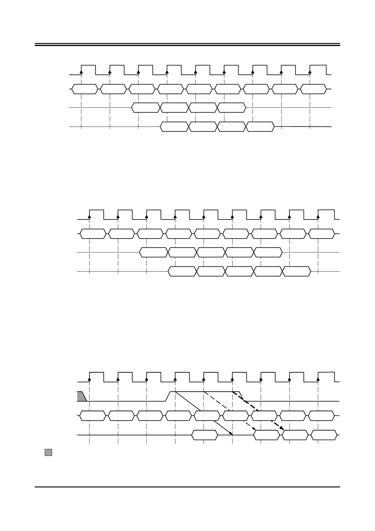
The DQM inputs are used to avoid I/O contention on the DQ pins when the interrupt comes
from a Write command. The DQMs must be asserted (HIGH) at least two clocks prior to the Write
command to suppress data-out on the DQ pins. To guarantee the DQ pins against I/O contention, a
single cycle with high-impedance on the DQ pins must occur between the last read data and the
Write command (refer to the following three figures). If the data output of the burst read occurs at the
second clock of the burst write, the DQMs must be asserted (HIGH) at least one clock prior to the
Write command to avoid internal bus contention.
T0
T1
T2
T3
T4
T5
T6
T7
T8
CLK
DQM
COMMAND
NOP
READ A
NOP
NOP
NOP
NOP
WRITE B
NOP
DQ's
: "H" or "L"
DOUT A0
Must be Hi-Z before
the Write Command
DINB0
DINB1
Read to Write Interval (Burst Length ≥ 4, CAS# Latency = 3)
NOP
DINB2
7
Rev 1.6 Feb. 2007
Share Link: 