HSP45240 데이터 시트보기 (PDF) - Intersil
부품명
상세내역
제조사
HSP45240 Datasheet PDF : 13 Pages
| |||
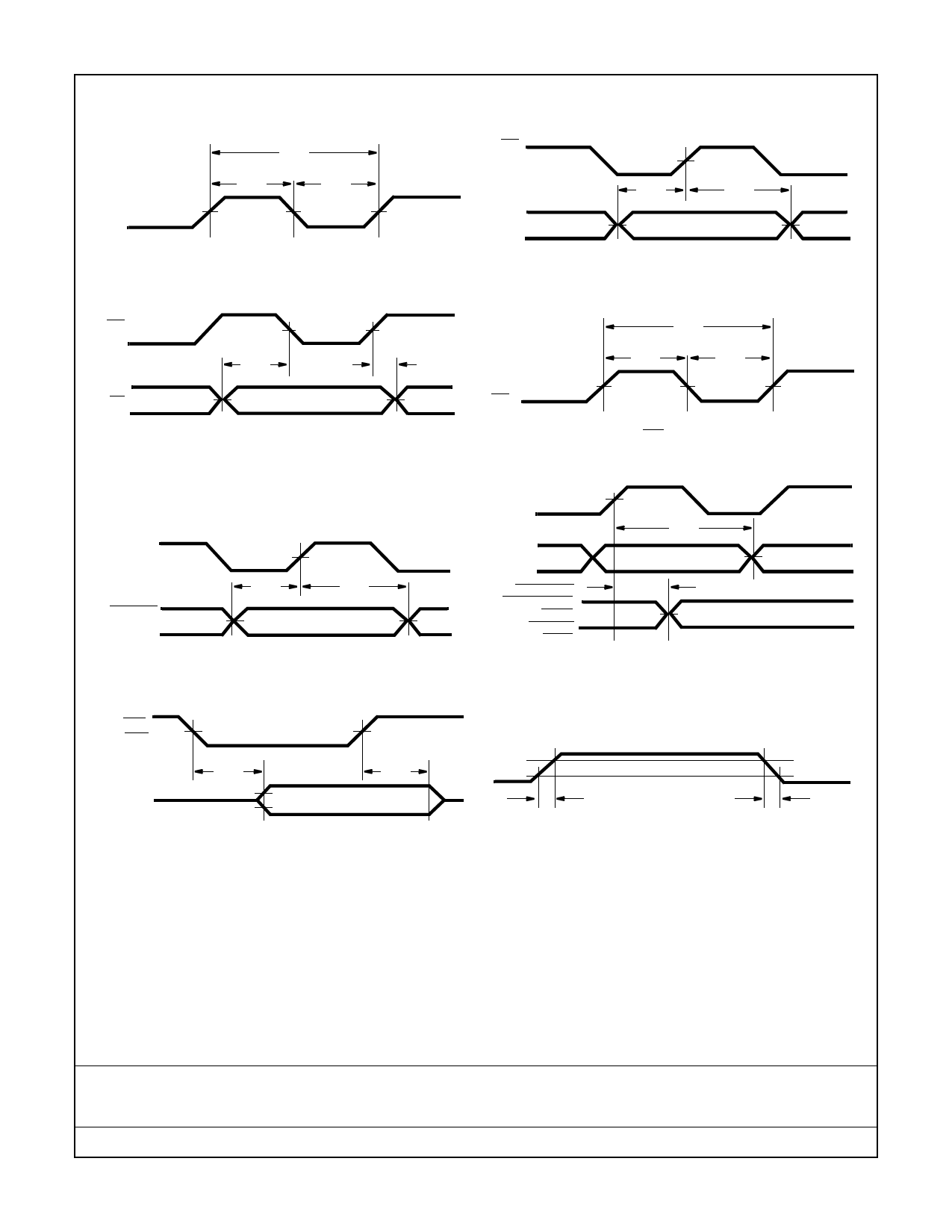
Timing Diagrams
tCP
tCH
tCL
CLK
FIGURE 8. CLOCK AC PARAMETERS
HSP45240
WR
D0-6
tDS
tDH
FIGURE 9. DATA SETUP AND HOLD
WR
tAS
A0,
CS
tAH
WR
FIGURE 10. ADDRESS/CHIP SELECT SETUP AND HOLD
tWP
tWRH
tWRL
FIGURE 11. WR AC PARAMETERS
CLK
STARTIN
DLYBLK
tIS
tIH
FIGURE 12. INPUT SET AND HOLD
OEL,
OEH
tEN
tOD
OUT0 - 23
1.7V
1.3V
FIGURE 14. OUTPUT ENABLE, DISABLE TIMING
CLK
tPDO
OUTO - 23
STARTOUT
BLOCKDONE
DONE
ADDVAL
BUSY
tPDS
FIGURE 13. OUTPUT PROPAGATION DELAY
VIH
VIL
tORF
2.0V
0.8V
tORF
FIGURE 15. OUTPUT RISE AND FALL TIMING
All Intersil U.S. products are manufactured, assembled and tested utilizing ISO9000 quality systems.
Intersil Corporation’s quality certifications can be viewed at www.intersil.com/design/quality
Intersil products are sold by description only. Intersil Corporation reserves the right to make changes in circuit design, software and/or specifications at any time without
notice. Accordingly, the reader is cautioned to verify that data sheets are current before placing orders. Information furnished by Intersil is believed to be accurate and
reliable. However, no responsibility is assumed by Intersil or its subsidiaries for its use; nor for any infringements of patents or other rights of third parties which may result
from its use. No license is granted by implication or otherwise under any patent or patent rights of Intersil or its subsidiaries.
For information regarding Intersil Corporation and its products, see www.intersil.com
13
Share Link: 