ISL90810WIU8(2005) 데이터 시트보기 (PDF) - Intersil
부품명
상세내역
제조사
ISL90810WIU8 Datasheet PDF : 11 Pages
| |||
ISL90810
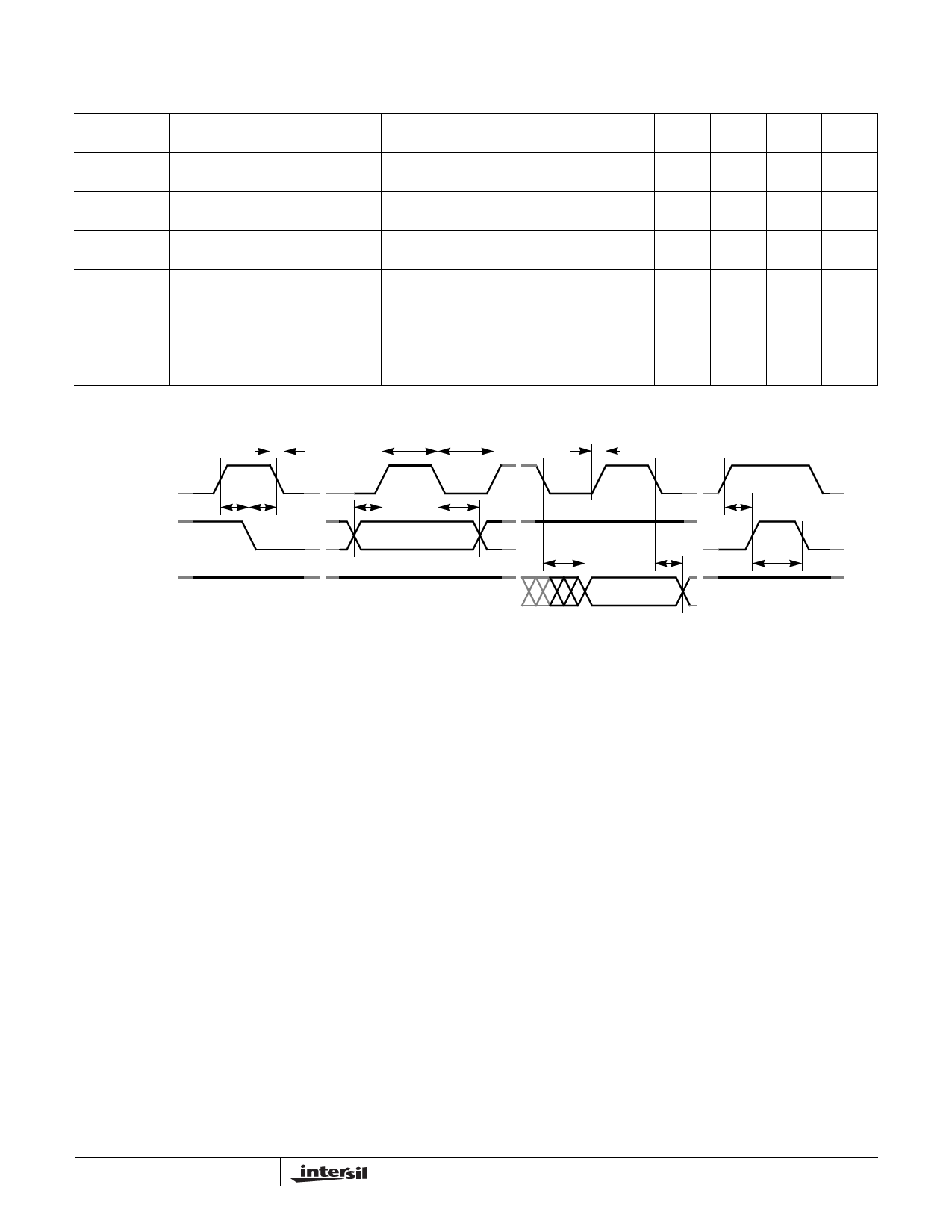
SDA vs SCL Timing
SCL
tSU:STA
SDA
(INPUT TIMING)
SDA
(OUTPUT TIMING)
tF
tHIGH
tSU:DAT
tHD:STA
tLOW
tHD:DAT
tR
tAA
tDH
tSU:STO
tBUF
NOTES:
1. Typical values are for TA = 25°C and 3.3V supply voltage.
2. LSB: [V(RW)255 – V(RW)0]/255. V(RW)255 and V(RW)0 are V(RW) for the DCP register set to FF hex and 00 hex respectively. LSB is the
incremental voltage when changing from one tap to an adjacent tap.
3. ZS error = V(RW)0/LSB.
4. FS error = [V(RW)255 – VCC]/LSB.
5. DNL = [V(RW)i – V(RW)i-1]/LSB-1, for i = 1 to 255. i is the DCP register setting.
6. INL = (V(RW)i – i • LSB – V(RW)0)/LSB, for i = 1 to 255.
7.
TCV
=
-------M-----a----x----(--V----(---R-----W------)--i--)---–-----M-----i--n----(--V-----(--R-----W------)--i--)------ × ----1----0---6-----
[Max(V(RW)i) + Min(V(RW)i)] ⁄ 2 125°C
for i = 16 to 240 decimal, T = -40°C to 85°C. Max( ) is the maximum value of the wiper
voltage and Min ( ) is the minimum value of the wiper voltage over the temperature range.
8. MI = |R255 – R0|/255. R255 and R0 are the measured resistances for the DCP register set to FF hex and 00 hex respectively.
Roffset = R0/MI, when measuring between RW and RL.
9. Roffset = R255/MI, when measuring between RW and RH.
10. RDNL = (Ri – Ri-1)/MI, for i = 32 to 255.
11. RINL = [Ri – (MI • i) – R0]/MI, for i = 32 to 255.
12.
TCR
=
----[---M-----a----x----(--R-----i--)---–-----M-----i--n----(--R-----i--)--]---- × ----1----0---6-----
[Max(Ri) + Min(Ri)] ⁄ 2 125°C
for i = 32 to 255, T = -40°C to 85°C. Max( ) is the maximum value of the resistance and Min ( ) is the
minimum value of the resistance over the temperature range.
13. This parameter is not 100% tested.
Equivalent Circuitry
RTOTAL
RH
RL
CL
CH
CW 10pF
10pF
25pF
RW
5
FN8234.1
October 13, 2005
Share Link: 