LH28F004SU-Z9 데이터 시트보기 (PDF) - Sharp Electronics
부품명
상세내역
제조사
LH28F004SU-Z9 Datasheet PDF : 31 Pages
| |||
4M (512K × 8) Flash Memory
LH28F004SU-Z9
The LH28F004SU contains a Compatible Status
Register (CSR) which is 100% compatible with the
LH28F008SA Flash memory’s Status Register.This reg-
ister, when used alone, provides a straightforward
upgrade capability to the LH28F004SU from a
LH28F008SA based design.
The LH28F004SU incorporates an open drain
RY »/BY » output pin. This feature allows the user to or-tie
many RY »/BY » pins together in a multiple memory con-
figuration such as a Resident Flash Array.
The LH28F004SU is specified for a maximum
access time of 150 ns (tACC) at 3.3 V operation (3.0 to
3.6 V) over the commercial temperature range (-20 to
+85°C). A corresponding maximum access time of
190 ns (tACC) at 2.7 V (-20 to +85°C) and 180 ns (tACC)
at 2.7 V (0 to +70°C) is achieved for reduced power
consumption applications.
The LH28F004SU incorporates an Automatic Power
Saving (APS) feature which substantially reduces the
active current when the device is in static mode of
operation (addresses not switching).
In APS mode, the typical ICC current is 1 mA at 3.3 V.
A Deep Power-Down mode of operation in invoked
when the RP » (called PWD on the LH28F008SA) pin
transitions low, any current operation is aborted and the
device is put into the deep power down mode. This mode
brings the device power consumption to less than 8 µa,
and provides additional write protection by acting as a
device reset pin during power transitions. When the
power is turned on, RP » pin is turned to low in order to
return the device to default configuration. When the
power transition has occurred, or at the power on/off,
RP » is required to stay low in order to protect data from
noise. A recovery time of 750 ns is required from RP »
switching high until outputs are again valid. In the Deep
Power-Down state, the WSM is reset (any current op-
eration will abort) and the CSR register is cleared.
A CMOS Standby mode of operation is enabled when
CE » transitions high and RP » stays high with all input
control pins at CMOS levels. In this mode, the device
draws an ICC standby current of 15 µA.
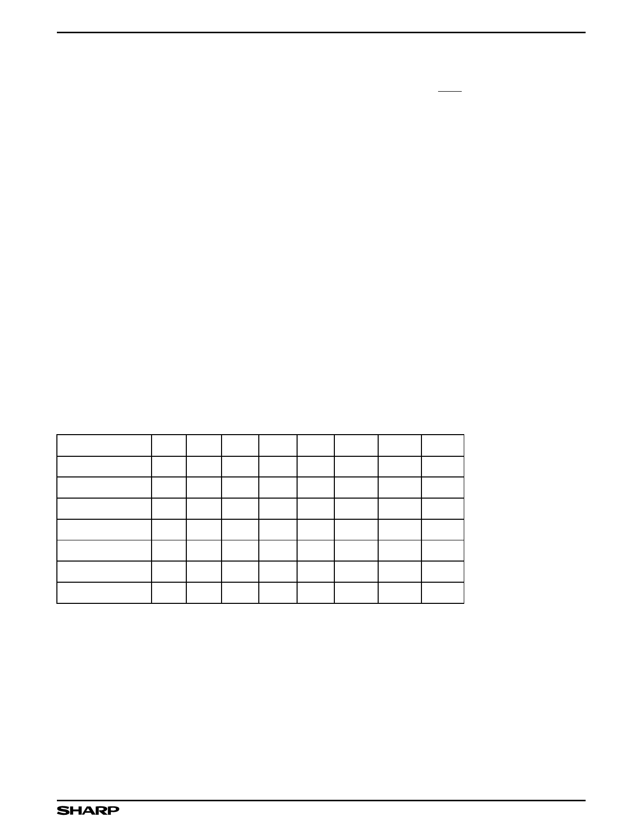
BUS OPERATIONS, COMMANDS AND
STATUS REGISTER DEFINITIONS
Bus Operations
MODE
RP » CE » OE »
WE
A0 DQ0-7 RY »/BY» NOTE
Read
VIH
VIL
VIL
VIH
X
DOUT
X 1, 2, 7
Output Disable
VIH
VIL
VIH
VIH
X High-Z X 1, 6, 7
Standby
VIH
VIH
X
X
X High-Z X 1, 6, 7
Deep Power-Down VIL
X
X
X
X High-Z VOH
1, 3
Manufacturer ID
VIH
VIL
VIL
VIH
VIL
B0H
VOH
4
Device ID
VIH
VIL
VIL
VIH
VIH
ID
VOH
4
Write
VIH
VIL
VIH
VIL
X
DIN
X 1, 5, 6
NOTES:
1. X can be VIH or VIL for address or control pins except for RY »/BY », which is either VOL or VOH.
2. RY »/BY » output is open drain. When the WSM is ready, Erase is suspended or the device is in deep
power-down mode, RY »/BY » will be at VOH if it is tied to VCC through a resistor. When the RY /» BY »
at VOL is independent of OE » while a WSM operation is in progress.
3. RP » at GND ± 0.2 V ensures the lowest deep power-down current.
4. A0 at VIL provide manufacturer ID codes. A0 at VIH provide device ID codes. Device ID code= 23H.
All other addresses are set to zero.
5. Commands for different Erase operations, Data Write operations, and Lock-Block operations can only
be successfully completed when VPP = VPPH.
6. While the WSM is running, RY »/BY » in Level-Mode (default) stays at VOL until all operations are complete.
RY »/BY » goes to VOH when the WSM is not busy or in erase suspend mode.
7. RY »/BY may be at VOL while the WSM is busy performing various operations. For example, a status register
read during a write operation.
5
Share Link: 