LMV981 데이터 시트보기 (PDF) - ON Semiconductor
부품명
상세내역
제조사
LMV981 Datasheet PDF : 21 Pages
| |||
LMV981, LMV982
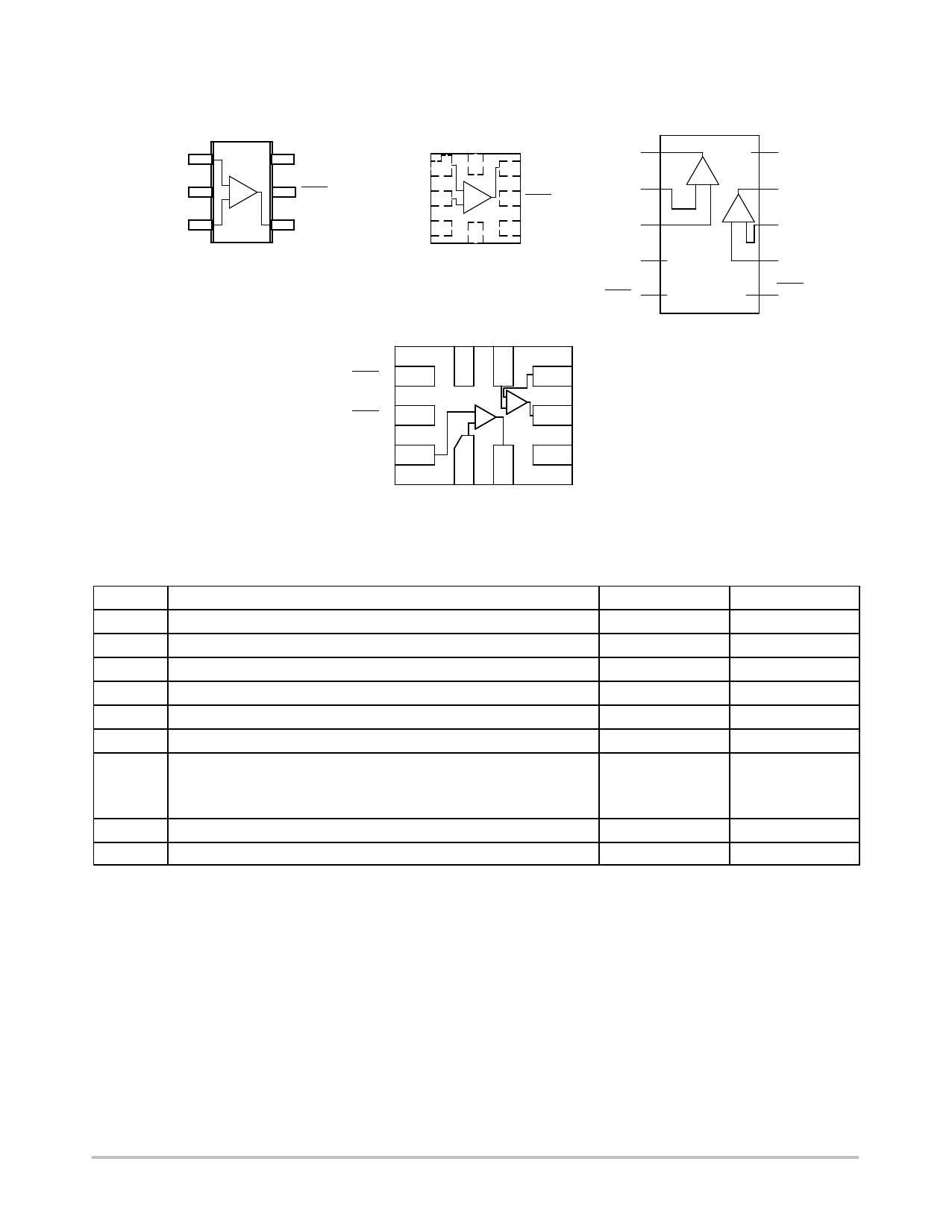
PIN CONNECTIONS
1
+IN
2
VEE
3
−IN
SC70−6
6
VCC
5
+
SHDN
−
4
OUT
(Top View)
ULLGA8/QFN
NC
IN− 1
8
7 OUT
+
IN+ 2
−
6 SHDN
VEE 3
4
5 VCC
NC
NC − No internal connection
(Top View)
UQFN10
VEE
+INA
SHDN A
8
SHDN B
9
7
6
5
−
+
+
−
4
OUT A 1
IN A− 2
IN A+ 3
VEE 4
SHDN A 5
−INA
OUTA
Micro10
A
−+
10 VCC
9 OUT B
B
+ − 8 IN B−
7 IN B+
6 SHDN B
(Top View)
+INB
10
1
2
−INB OUTB
(Top View)
3
VCC
MAXIMUM RATINGS
Symbol
Rating
Value
Unit
VS
VIDR
VICR
Supply Voltage (Operating Range VS = 2.7 V to 5.5 V)
Input Differential Voltage
Input Common Mode Voltage Range
Maximum Input Current
5.5
V
$Supply Voltage
V
−0.5 to (V+) + 0.5
V
10
mA
tSo
Output Short Circuit (Note 1)
TJ
Maximum Junction Temperature (Operating Range −40°C to 85°C)
qJA
Thermal Resistance
SC−70
ULLGA8
Micro10
UQFN10
Continuous
150
280
340
200
300
°C
°C/W
Tstg
Storage Temperature (SOT23−6)
Mounting Temperature (Infrared or Convection −30 sec)
−65 to 150
°C
260
°C
Stresses exceeding Maximum Ratings may damage the device. Maximum Ratings are stress ratings only. Functional operation above the
Recommended Operating Conditions is not implied. Extended exposure to stresses above the Recommended Operating Conditions may
affect device reliability.
ESD data available upon request.
1. Continuous short−circuit operation to ground at elevated ambient temperature can result in exceeding the maximum allowed junction
temperature of 150°C. Output currents in excess of 45 mA over long term may adversely affect reliability. Shorting output to either V+
or V− will adversely affect reliability.
http://onsemi.com
2
Share Link: 