LTC1410 데이터 시트보기 (PDF) - Linear Technology
부품명
상세내역
제조사
LTC1410 Datasheet PDF : 16 Pages
| |||
LTC1410
APPLICATIONS INFORMATION
where V1 is the RMS amplitude of the fundamental fre-
quency and V2 through Vn are the amplitudes of the
second through nth harmonics. THD vs Input Frequency is
shown in Figure 4. The LTC1410 has good distortion
performance up to the Nyquist frequency and beyond.
0
–10
–20
–30
–40
–50
–60
–70
–80
–90
–100
1k
3RD THD
2ND
10k
100k
1M
INPUT FREQUENCY (Hz)
10M
1410 G03
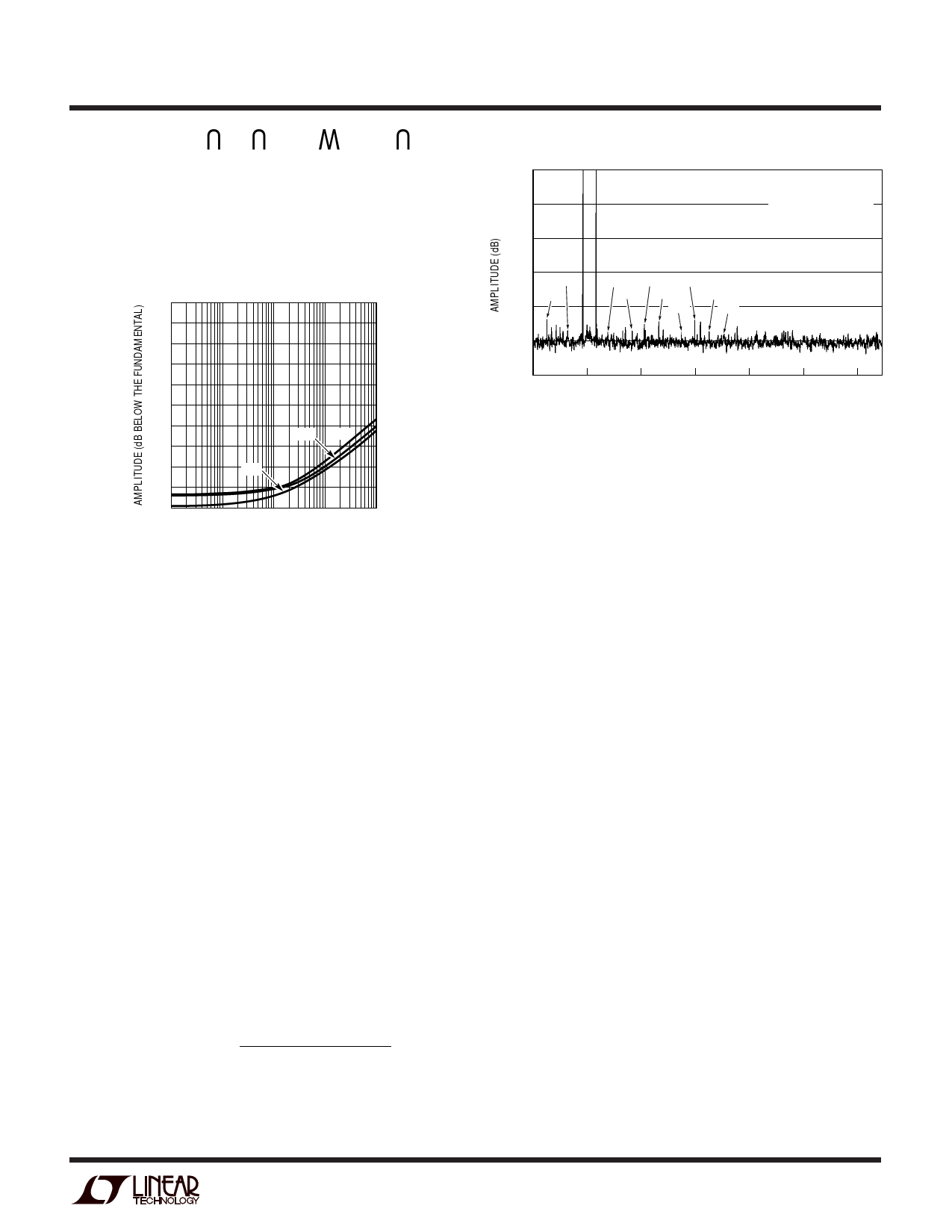
Figure 4. Distortion vs Input Frequency
Intermodulation Distortion (IMD)
If the ADC input signal consists of more than one spectral
component, the ADC transfer function nonlinearity can
produce Intermodulation Distortion in addition to THD.
IMD is the change in one sinusoidal input caused by the
presence of another sinusoidal input at a different
frequency.
If two pure sine waves of frequencies fa and fb are applied
to the ADC input, nonlinearities in the ADC transfer func-
tion can create distortion products at the sum and differ-
ence frequencies of mfa ± nfb, where m and n = 0, 1, 2, 3,
etc. For example, the 2nd order IMD terms include
(fa + fb). If the two input sine waves are equal in magnitude,
the value (in decibels) of the 2nd order IMD products can
be expressed by the following formula:
( ) ( ) IMD
fa + fb
Amplitude at
= 20 log
fa ± fb
Amplitude at fa
0
(fa) (fb)
–20
–40
fSAMPLE = 1.25MHz
fIN1 = 88.19580078kHz
fIN2 = 111.9995117kHz
–60 (2fa–fb)
(fb–fa)
–80
(2fb–fa) (fa+fb) (2fa+fb)
(2fa) (2fb) (fa+2fb)
(3fa)
(3fb)
–100
–120
0
100
200
300
400
500
600
FREQUENCY (MHz)
1410 F05
Figure 5. Intermodulation Distortion Plot
Peak Harmonic or Spurious Noise
The peak harmonic or spurious noise is the largest spec-
tral component excluding the input signal and DC. This
value is expressed in decibel relative to the RMS value of
a full-scale input signal.
Full Power and Full Linear Bandwidth
The full power bandwidth is that input frequency at which
the amplitude of the reconstructed fundamental is re-
duced by 3dB for a full-scale input signal.
The full linear bandwidth is the input frequency at which
the S/(N + D) has dropped to 68dB (11 effective bits). The
LTC1410 has been designed to optimize input bandwidth,
allowing the ADC to undersample input signals with fre-
quencies above the converter’s Nyquist frequency. The
noise floor stays very low at high frequencies; S/(N + D)
does not become dominated by distortion until frequen-
cies far beyond Nyquist.
Driving the Analog Input
The differential analog inputs of the LTC1410 are easy to
drive. The inputs may be driven differentially or as a
single-ended input (i.e., the – AIN input is grounded). The
+ AIN and – AIN inputs are sampled at the same instant.
Any unwanted signal that is common mode to both
inputs will be reduced by the common mode rejection of
the sample-and-hold circuit. The inputs draw only one
small current spike while charging the sample-and-hold
9
Share Link: 