LTC4310IMS-1 데이터 시트보기 (PDF) - Linear Technology
부품명
상세내역
제조사
LTC4310IMS-1 Datasheet PDF : 20 Pages
| |||
LTC4310-1/LTC4310-2
Applications Information
Once a STOP bit or bus idle occurs on both the local and
isolated buses, the LTC4310 reactivates its buffers and
rise time accelerators.
READY Digital Output
The READY pin provides a digital output flag that pulls
low to indicate that the LTC4310 is driving its SDA and
SCL pins with the logic state information it is receiving on
its RXP and RXN pins from the other LTC4310. READY is
driven by an N-channel MOSFET open-drain pull-down that
is capable of sinking 4mA while holding 0.4V maximum.
The pull-down turns off whenever the LTC4310 is not
driving its SDA and SCL pins—during start-up, thermal
shutdown, low current shutdown and after disconnection
due to a stuck bus or failure to receive a transmission
within 4.6ms. Connect a resistor to the bus pull-up supply
to provide the pull-up.
Design Example: High Voltage Isolation Using an
Inexpensive Ethernet Transformer
Figure 1 shows the LTC4310-1 providing I2C communi-
cations between two buses whose ground voltages can
differ up to 1500V. An EPF8119S Ethernet transformer is
used to bridge the isolation barrier. The left I2C bus con-
nects to the LTC4310-1 and two other devices, resulting
in a bus parasitic capacitance of 40pF in this example
set-up. Referring to the VCC = 3.3V curve in Figure 2,
7.5k pull-up resistors are chosen for R1 and R2. The right
I2C bus connects to another LTC4310-1 and four slave
devices, resulting in a bus parasitic capacitance of 80pF.
Referring to the VCC = 5V curve in Figure 2, 7.5k pull-up
resistors are also chosen for R5 and R6. Standard 5%
resistors are used.
Sudden changes in the ground differential across the
isolation barrier can be effectively resisted by tying the
center tap of the receive side of the transformer to the
local ground through a 0.01µF capacitor, as shown by
capacitors C2 and C3.
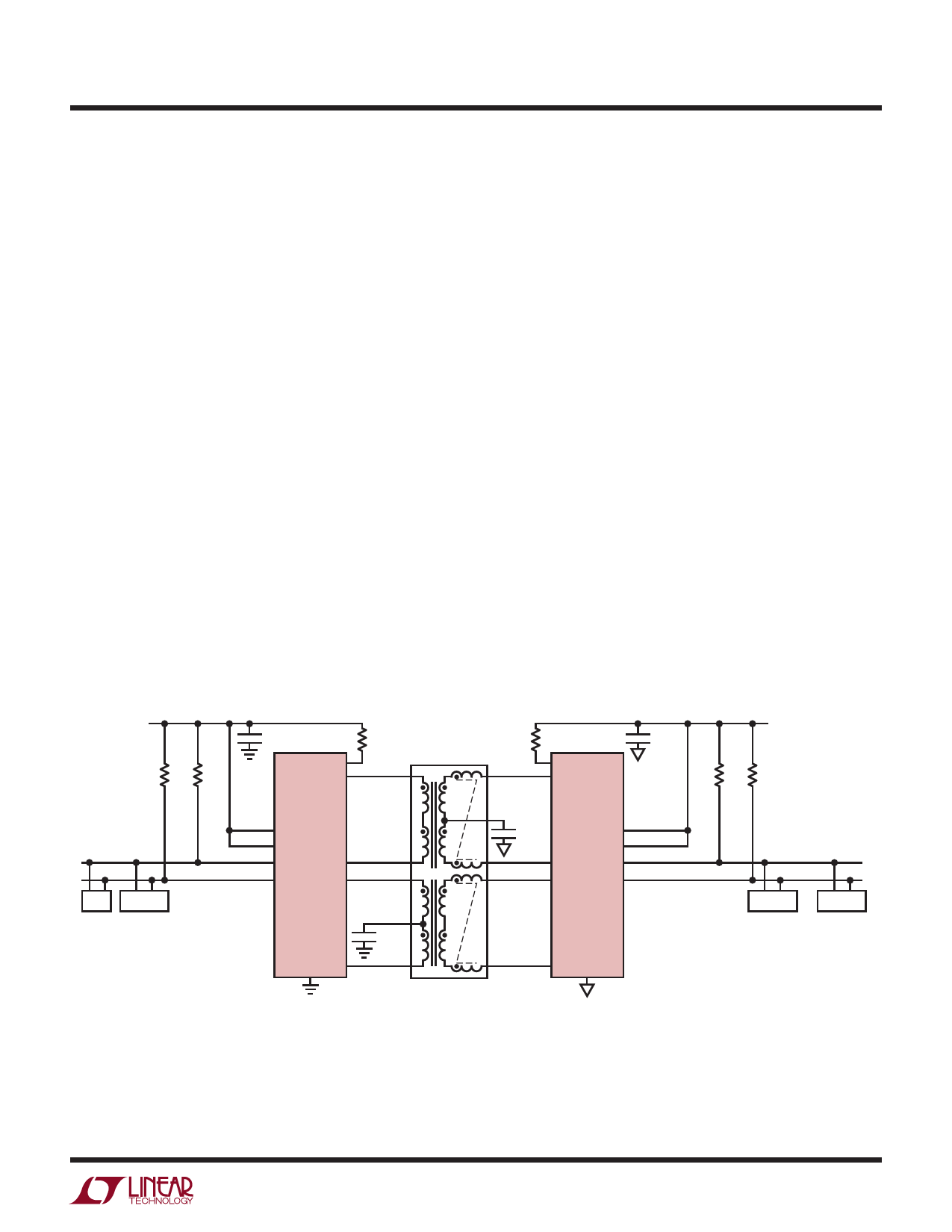
Figure 7 shows the same application as Figure 1, but with
each LTC4310-1 replaced by an LTC4310-2, so that the
bus can switch at frequencies up to 400kHz. To meet the
requirements shown in the curves of Figure 3, R1 and R2
are changed from 7.5k to 4.3k, and R5 and R6 are changed
from 7.5k to 3.3k.
3.3V
R1 R2
4.3k 4.3k
C1
0.01µF
READY
TXP
LTC4310-2
CBUS = 40pF
µP
SLAVE
VCC
EN
SDA TXN
SCL1
SCL
RXP
GND RXN
R3
10/100Base-TX
10k
ETHERNET
TRANSFORMER
1
16
R4
10k
READY
RXP
15
LTC4310-2
C3
0.01µF
VCC
EN
3
14
RXN SDA
6
11
TXP
SCL
C4
0.01µF
SCL2
7
C2
0.01µF
8
9
EPF8119S
TXN GND
431012 F07
Figure 7. The LTC4310-2 in a 400kHz Application
IS0LATED
5V
R5 R6
3.3k 3.3k
CBUS = 80pF
SLAVE#1 . . . SLAVE#4
431012fa
13
Share Link: 