MAX9879 데이터 시트보기 (PDF) - Maxim Integrated
부품명
상세내역
제조사
MAX9879 Datasheet PDF : 32 Pages
| |||
MAX9879
Stereo Class D Audio Subsystem
with DirectDrive Headphone Amplifier
1) The sleeve is typically grounded to the chassis.
Using the midrail biasing approach, the sleeve
must be isolated from system ground, complicating
product design.
2) During an ESD strike, the amplifier’s ESD structures
are the only path to system ground. Thus, the
amplifier must be able to withstand the full energy
from an ESD strike.
3) When using the headphone jack as a line out to
other equipment, the bias voltage on the sleeve
may conflict with the ground potential from other
equipment, resulting in possible damage to the
amplifiers.
The MAX9879 features a low-noise charge pump. The
switching frequency of the charge pump is 1/2 of the
Class D switching frequency, regardless of the operating
mode. Since the Class D amplifiers are operated in
spread-spectrum mode, the charge pump also switches
with a spread-spectrum pattern. The nominal switching
frequency is well beyond the audio range, and thus does
not interfere with audio signals. The switch drivers fea-
ture a controlled switching speed that minimizes noise
generated by turn-on and turn-off transients. By limiting
the switching speed of the charge pump, the di/dt noise
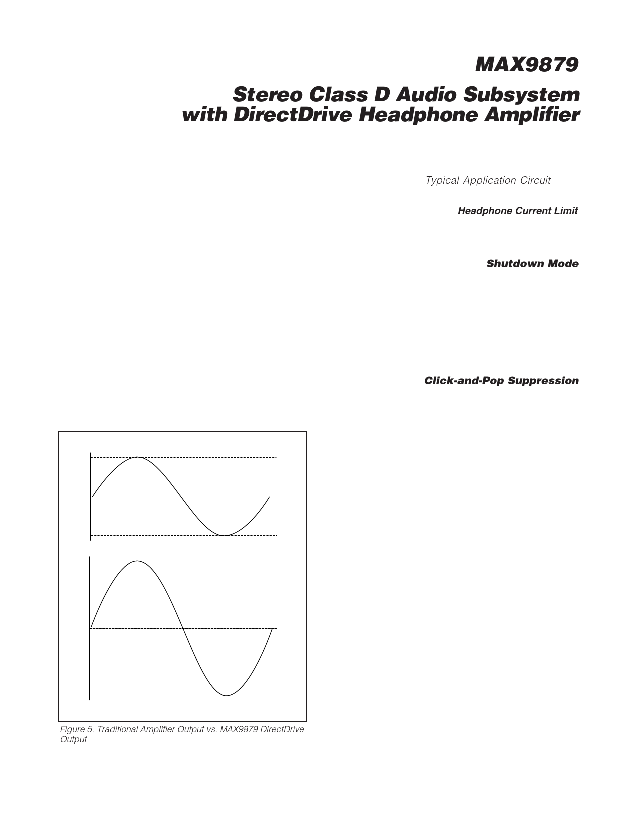
VDD
VOUT
VDD/2
GND
CONVENTIONAL DRIVER BIASING SCHEME
+VDD
VOUT
GND
-VDD
DirectDrive BIASING SCHEME
Figure 5. Traditional Amplifier Output vs. MAX9879 DirectDrive
Output
Maxim Integrated
caused by the parasitic trace inductance is minimized.
Although not typically required, additional high-frequen-
cy noise attenuation can be achieved by increasing the
size of C2 (see the Typical Application Circuit). The
charge pump is active only in headphone modes.
Headphone Current Limit
The headphone amplifier current is limited to 140mA (typ).
The current limit clamps the output current, which appears
as clipping when the maximum current is exceeded.
Shutdown Mode
The MAX9879 features two ways of entering low-power
shutdown:
• The device can be placed in shutdown mode by writ-
ing to the SHDN bit in the Output Control Register.
• The device can be placed in an ultra-low power shut-
down mode by setting the SHDN pin to 0V. This com-
pletely disables the MAX9879 including the I2C
interface.
Click-and-Pop Suppression
The MAX9879 features click-and-pop suppression that
eliminates audible transients from occurring at startup
and shutdown.
Use the following procedure to start up the MAX9879:
1) Configure the desired output mode and pream-
plifier gain.
2) Set the SHDN bit to 1 to start up the amplifier.
3) Wait 10ms for the startup time to pass.
4) Increase the output volume to the desired level.
To disable the device simply set SHDN to 0.
During the startup period, the MAX9879 precharges the
input capacitors to prevent clicks and pops. If the output
amplifiers have been programmed to be active they are
held in shutdown until the precharge period is complete.
When power is initially applied to the MAX9879, the
power-on-reset state of all three volume control registers
is mute. For most applications, the volume can be set to
the desired level once the device is active. If the click-
and-pop is too high, step through intermediate volume
settings with zero-crossing detection disabled. Stepping
through higher volume settings has a greater impact on
click-and-pop than lower volume settings.
For the lowest possible click and pop, start up the device
at minimum volume and then step through each volume
setting until the desired setting is reached. Disable zero-
crossing detection if no input signal is expected.
21
Share Link: 