MCF51JE128 데이터 시트보기 (PDF) - Freescale Semiconductor
부품명
상세내역
제조사
MCF51JE128 Datasheet PDF : 47 Pages
| |||
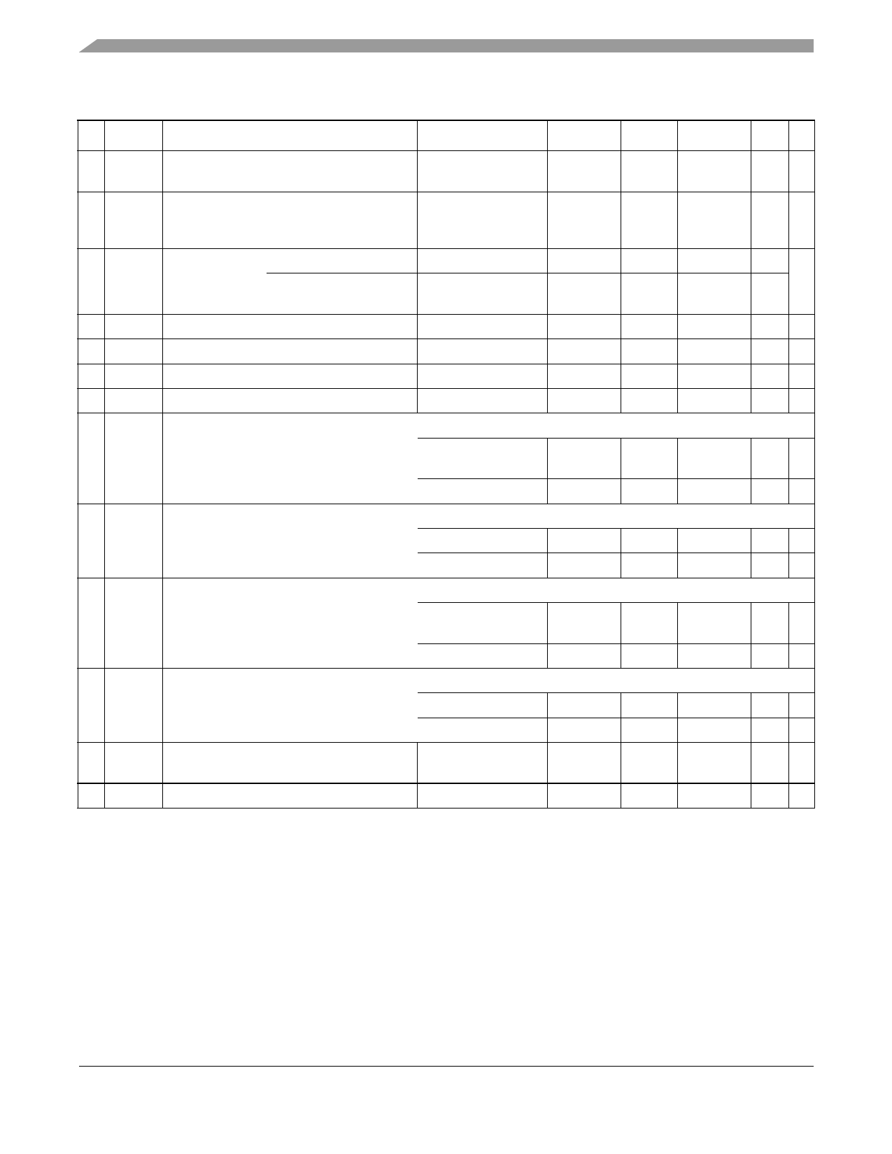
Preliminary Electrical Characteristics
Table 9. DC Characteristics (continued)
# Symbol
Characteristic
Condition
Minimum Typical1 Maximum Unit C
11 RPU Pull-up resistors
all digital inputs, when
enabled
—
12
Internal
RPD pull-down
—
resistors4
13
IIC
DC injection
current 5, 6, 7
Single pin limit
Total MCU limit, includes
sum of all stressed pins
VSS > VIN > VDD
VSS > VIN > VDD
14 CIn Input Capacitance, all pins
—
15 VRAM RAM retention voltage
—
16 VPOR POR re-arm voltage8
—
17 tPOR POR re-arm time
—
18 VLVDH Low-voltage detection threshold — high range9
VDD falling
17.5
—
17.5
—
–0.2
—
–5
—
—
—
—
0.6
0.9
1.4
10
—
2.11
2.16
52.5
k P
52.5
k P
0.2
mA
D
5
mA
8
pF C
1.0
VC
1.79
VC
—
s D
2.22
VP
VDD rising
19 VLVDL Low-voltage detection threshold — low range9
VDD falling
20 VLVWH Low-voltage warning threshold — high range9
VDD rising
VDD falling
2.16
2.21
2.27
VP
1.80
1.82
1.91
VP
1.86
1.90
1.99
VP
2.36
2.46
2.56
VP
21 VLVWL Low-voltage warning threshold — low range9
VDD rising
2.36
2.46
2.56
VP
VDD falling
2.11
2.16
2.22
VP
VDD rising
2.16
2.21
2.27
VP
22
Vhys
Low-voltage inhibit reset/recover
hysteresis10
—
—
50
—
mV C
23 VBG Bandgap Voltage Reference11
—
1.145
1.17
1.195
VP
1 Typical values are measured at 25C. Characterized, not tested
2 As the supply voltage rises, the LVD circuit will hold the MCU in reset until the supply has risen above VLVDL.
3 Does not include analog module pins. Dedicated analog pins should not be pulled to VDD or VSS and should be left floating when not used
to reduce current leakage.
4 Measured with VIn = VDD.
5 All functional non-supply pins are internally clamped to VSS and VDD,except PTD1.
6 Input must be current limited to the value specified. To determine the value of the required current-limiting resistor, calculate resistance values
for positive and negative clamp voltages, then use the larger of the two values.
7 Power supply must maintain regulation within operating VDD range during instantaneous and operating maximum current conditions. If positive
injection current (VIn > VDD) is greater than IDD, the injection current may flow out of VDD and could result in external power supply going out
of regulation. Ensure external VDD load will shunt current greater than maximum injection current. This will be the greatest risk when the MCU
is not consuming power. Examples are: if no system clock is present, or if clock rate is very low (which would reduce overall power
consumption).
MCF51JE256 Datasheet, Rev. 4
20
Freescale Semiconductor
Share Link: 