MCP16321 데이터 시트보기 (PDF) - Microchip Technology
부품명
상세내역
제조사
MCP16321
Microchip Technology
MCP16321 Datasheet PDF : 34 Pages
| |||
5.0 APPLICATION INFORMATION
5.0.1 TYPICAL APPLICATIONS
The MCP16321/2 synchronous step-down converter
operates over a wide input range, up to 24V maximum.
Typical applications include generating a bias or VDD
voltage for PIC® microcontrollers, digital control system
bias supply for AC-DC converters and 12V industrial
input and similar applications.
5.0.2
ADJUSTABLE OUTPUT VOLTAGE
CALCULATIONS
To calculate the resistor divider values for the
MCP16321/2 adjustable version, use Equation 5-1.
RTOP is connected to VOUT, RBOT is connected to
SGND, and both are connected to the VFB input pin.
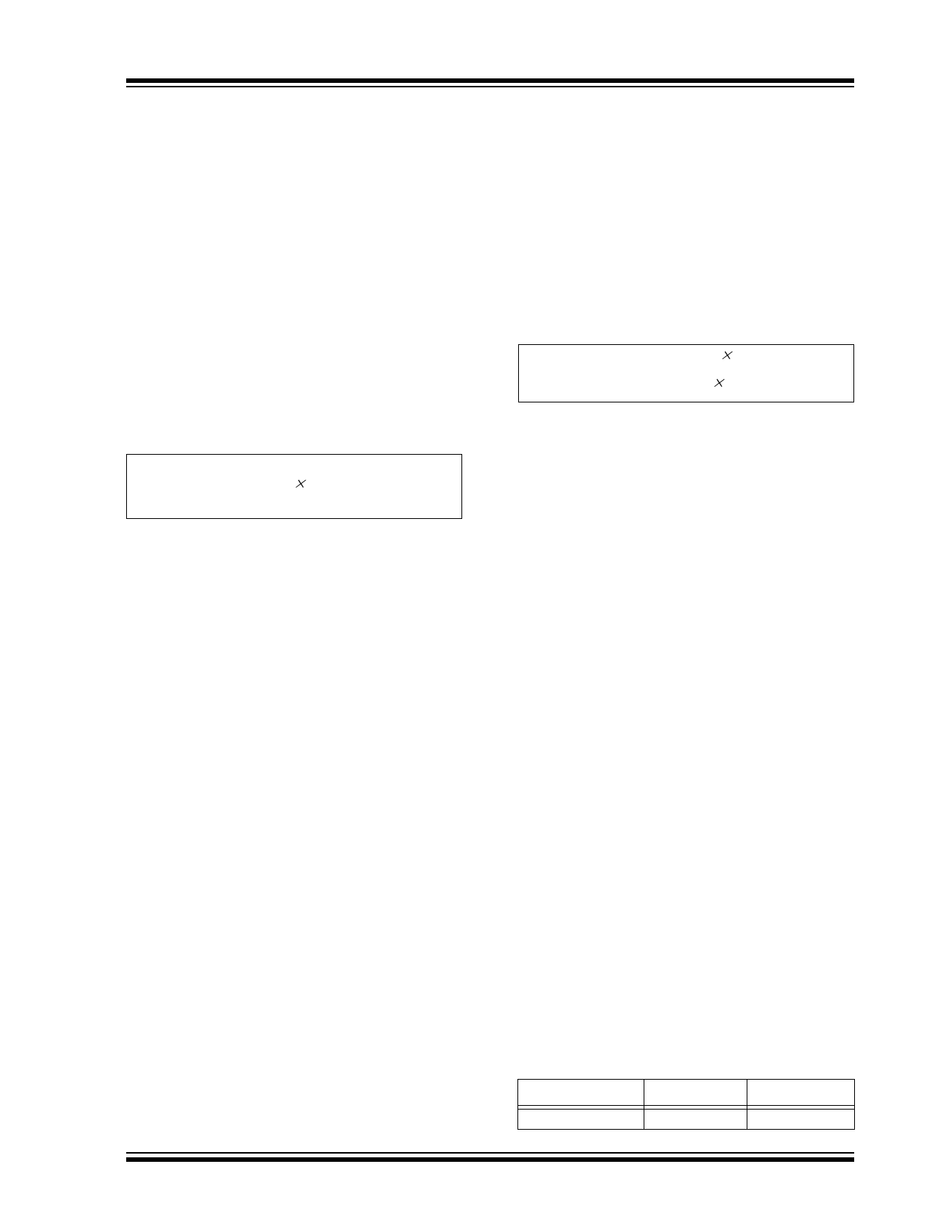
EQUATION 5-1: RESISTOR DIVIDER
CALCULATION
VOUT
=
VFB
×
⎝⎛1
+
R----T---O----P-
RBOT
⎞
⎠
EXAMPLE 5-1: 2.0V RESISTOR DIVIDER
VOUT = 2.0V
VFB = 0.9V
RBOT = 10 kΩ
RTOP = 12.2 kΩ (standard value = 12.3 kΩ)
VOUT = 2.007V (using standard values)
EXAMPLE 5-2: 4.2V RESISTOR DIVIDER
VOUT = 4.2V
VFB = 0.9V
RBOT = 10 kΩ
RTOP = 36.7 kΩ (standard value = 36.5 kΩ)
VOUT = 4.185V (using standard values)
The error amplifier is internally compensated to ensure
loop stability. External resistor dividers, inductance and
output capacitance, all have an impact on the control
system and should be selected carefully and evaluated
for stability. A 10 kΩ resistor is recommended as a
good trade-off for quiescent current and noise
immunity.
© 2011 Microchip Technology Inc.
MCP16321/2
5.0.3 GENERAL DESIGN EQUATIONS
The step-down converter duty cycle can be estimated
using Equation 5-2 while operating in Continuous
Inductor Current Mode. This equation accounts for the
forward drop of two internal N-Channel MOSFETS. As
load current increases, the voltage drop in both internal
switches will increase, requiring a larger PWM duty
cycle to maintain the output voltage regulation. Switch
voltage drop is estimated by multiplying the switch
current times the switch resistance or RDSON.
EQUATION 5-2: CONTINUOUS INDUCTOR
CURRENT DUTY CYCLE
D = -V-V--O--I--UN---T-–---+--(--I-(--H-I--LS---WS--W---×--×---R--R--D--D-S---OS--O-N---NH---L-)--)
5.0.4 INPUT CAPACITOR SELECTION
The step-down converter input capacitor must filter the
high-input ripple current, as a result of pulsing or
chopping the input voltage. The MCP16321/2 input
voltage pin is used to supply voltage for the power train
and as a source for internal bias. A low equivalent
series resistance (ESR), preferably a ceramic
capacitor, is recommended. The necessary
capacitance is dependent upon the maximum load
current and source impedance. Three capacitor
parameters to keep in mind are the voltage rating,
equivalent series resistance and the temperature
rating. For wide temperature range applications, a
multilayer X7R dielectric is recommended, while for
applications with limited temperature range, a
multilayer X5R dielectric is acceptable. The input
capacitor voltage rating must be VIN plus margin.
5.0.5 OUTPUT CAPACITOR SELECTION
The output capacitor provides a stable output voltage
during sudden load transients, and reduces the output
voltage ripple. As with the input capacitor, X5R and
X7R ceramic capacitors are well suited for this applica-
tion.
The MCP16321/2 is internally compensated, so the
output capacitance range is limited. See TABLE 5-1:
“Capacitor Value Range” for the recommended out-
put capacitor range.
The amount and type of output capacitance and
equivalent series resistance will have a significant
effect on the output ripple voltage and system stability.
The range of the output capacitance is limited due to
the integrated compensation of the MCP16321/2.
The output voltage capacitor rating should be a
minimum of VOUT plus margin.
TABLE 5-1: CAPACITOR VALUE RANGE
Parameter
Min
Max
CIN
8 µF
None
DS22285A-page 19
Share Link: 