NCV8440 데이터 시트보기 (PDF) - ON Semiconductor
부품명
상세내역
제조사
NCV8440 Datasheet PDF : 11 Pages
| |||
NCV8440, NCV8440A
MAXIMUM RATINGS (TJ = 25°C unless otherwise noted)
Rating
Symbol
Value
Unit
Drain−to−Source Voltage Internally Clamped
Gate−to−Source Voltage − Continuous
Drain Current
Total Power Dissipation @ TA = 25°C (Note 1)
Operating and Storage Temperature Range
− Continuous @ TA = 25°C
− Single Pulse (tp = 10 ms) (Note 1)
Single Pulse Drain−to−Source Avalanche Energy
(VDD = 50 V, ID(pk) = 1.17 A, VGS = 10 V, L = 160 mH, RG = 25 W)
VDSS
VGS
ID
IDM
PD
TJ, Tstg
EAS
52−59
V
±15
V
2.6
A
10
1.69
W
−55 to 150
°C
110
mJ
Load Dump Voltage (VGS = 0 and 10 V, RI = 2.0 W, RL = 9.0 W, td = 400 ms)
Thermal Resistance,
Junction−to−Ambient (Note 1)
Junction−to−Ambient (Note 2)
Maximum Lead Temperature for Soldering
Purposes, 1/8″ from Case for 10 Seconds
VLD
RqJA
RqJA
TL
60
V
°C/W
74
169
260
°C
Stresses exceeding those listed in the Maximum Ratings table may damage the device. If any of these limits are exceeded, device functionality
should not be assumed, damage may occur and reliability may be affected.
1. When surface mounted to a FR4 board using 1″ pad size, (Cu area 1.127 in2).
2. When surface mounted to a FR4 board using minimum recommended pad size, (Cu area 0.412 in2).
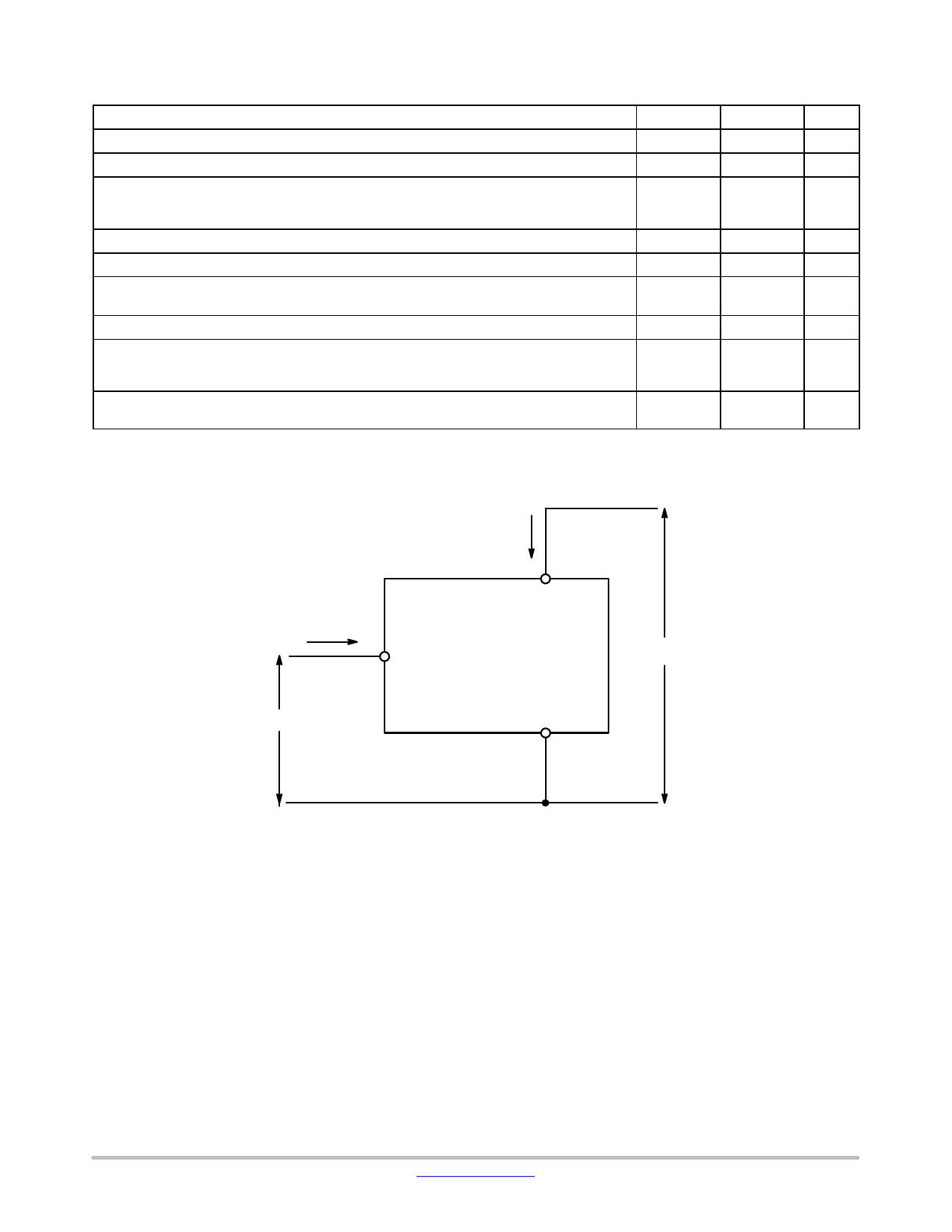
+
ID
IG
+
VGS
GATE
DRAIN
SOURCE
VDS
−
−
Figure 1. Voltage and Current Convention
www.onsemi.com
2
Share Link: 