RT8057GQW 데이터 시트보기 (PDF) - Richtek Technology
부품명
상세내역
제조사
RT8057GQW Datasheet PDF : 11 Pages
| |||
RT8057
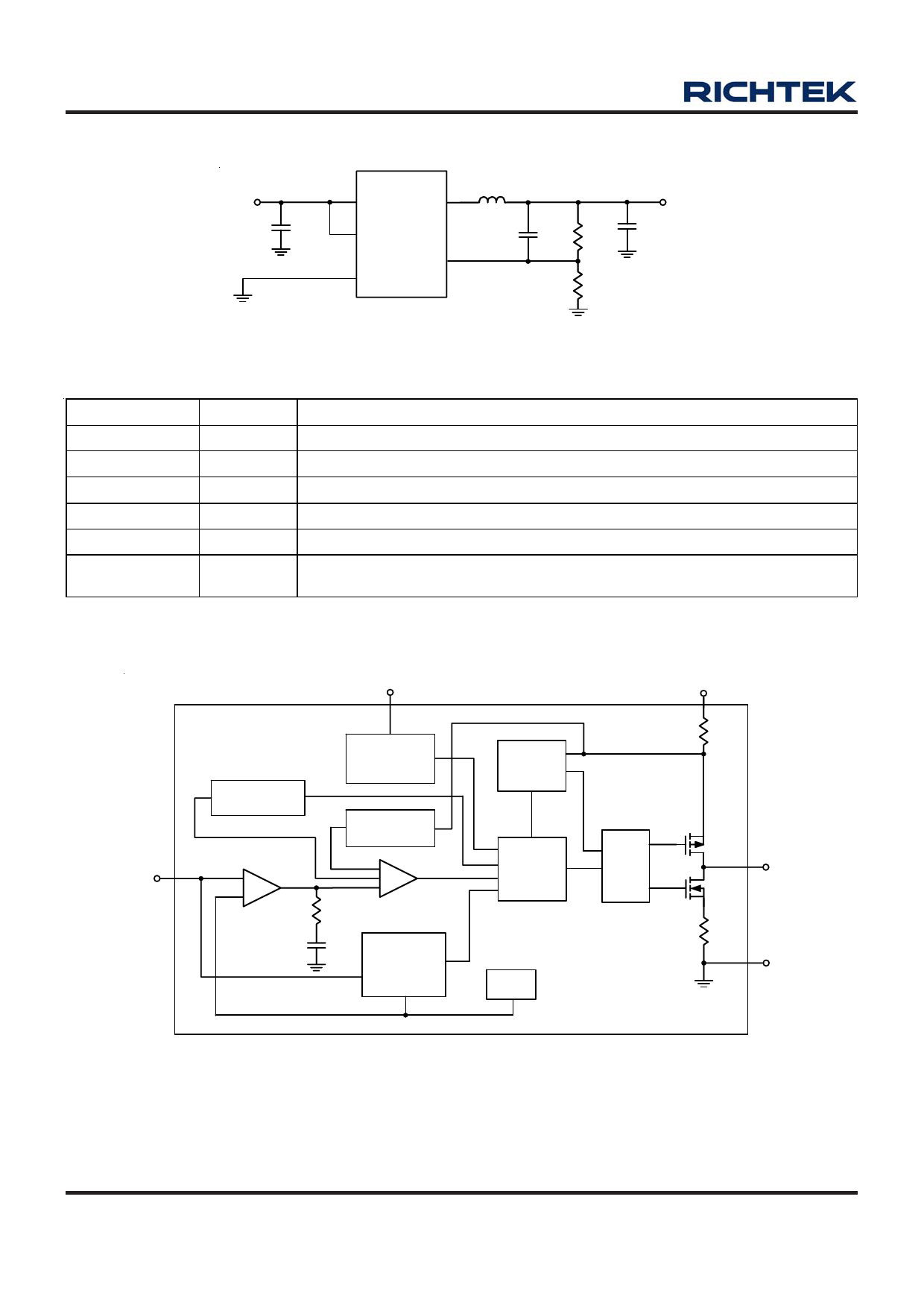
Typical Application Circuit
RT8057
VIN
5 VIN
LX 1
CIN
4.7µF
4 EN
6, 7 (Exposed Pad)
GND
3
FB
L1
2.2µH
C1 R1
10pF 680k
R2
240k
VOUT
2.3V
COUT
10µF
Function Pin Description
Pin No.
Pin Name
Pin Function
1
LX
Switch Node. Connect to the external inductor.
2
NC
3
FB
4
EN
No Internal Connection. Connect to GND.
Feedback Pin. Connect to the external resistor divider.
Chip Enable (Active High).
5
VIN
6,
7 (Exposed Pad)
GND
Power Input. Connect to the input capacitor.
Power GND. The Exposed Pad must be soldered to a large PCB and connected
to GND for maximum power dissipation.
Function Block Diagram
EN
Slope
Compensation
OSC &
Shutdown
Control
Current
Sense
Error
Amplifier
FB
PWM
RC
Comparator
COMP
UVLO &
Power Good
Detector
Current
Limit
Detector
Control
Logic
VREF
VIN
RS1
Driver
LX
RS2
GND
www.richtek.com
2
DS8057-03 November 2011
Share Link: 