S34ML01G104THI010 데이터 시트보기 (PDF) - Spansion Inc.
부품명
상세내역
제조사
S34ML01G104THI010 Datasheet PDF : 73 Pages
| |||
Data Sheet (Preliminary)
1.6.3
S34ML04G1
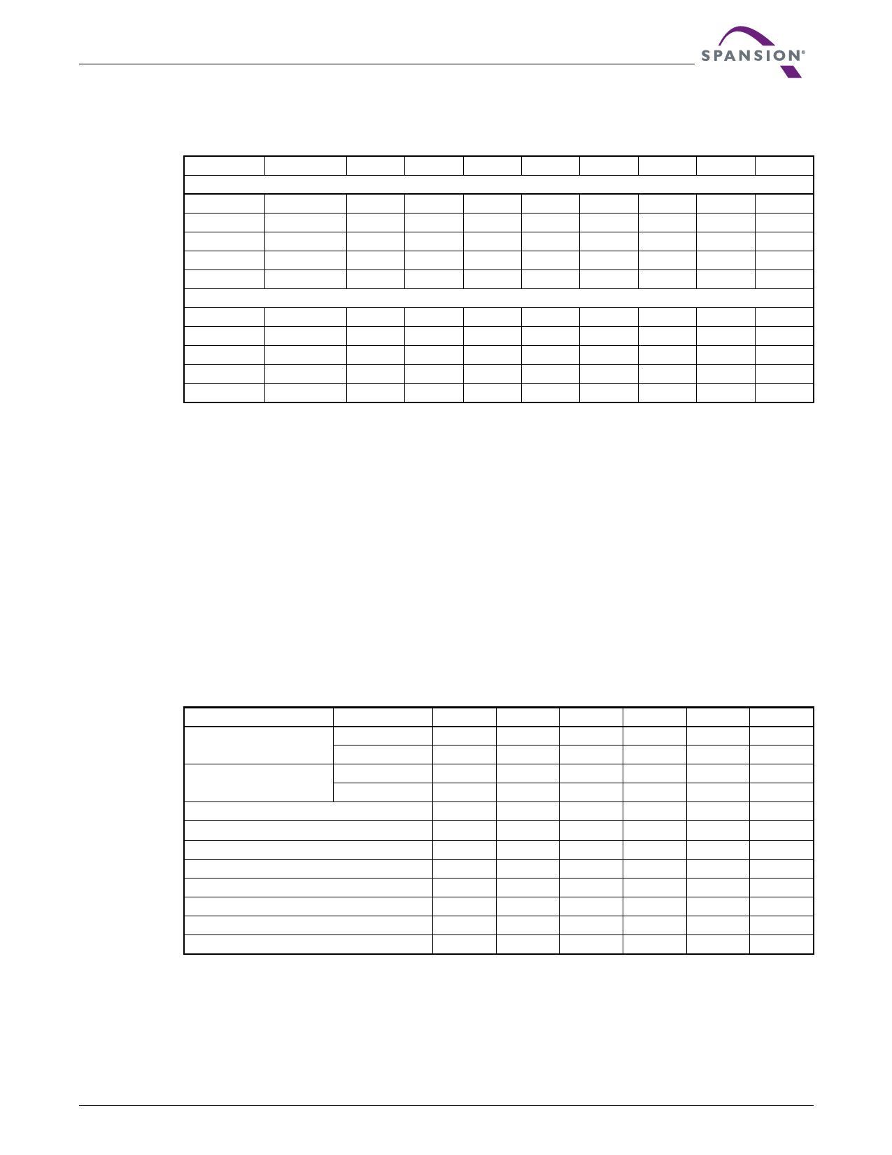
Table 1.5 Address Cycle Map — 4 Gb Device
Bus Cycle
I/O [15:8] (3)
I/O0
I/O1
I/O2
I/O3
x8
1st
—
A0
A1
A2
A3
2nd
—
A8
A9
A10
A11
3rd
—
A12
A13
A14
A15
4th
—
A20
A21
A22
A23
5th
—
A28
A29
A30
L (1)
x16
1st
Low
A0
A1
A2
A3
2nd
Low
A8
A9
A10
L (2)
3rd
Low
A11
A12
A13
A14
4th
Low
A19
A20
A21
A22
5th
Low
A27
A28
A29
L (2)
Notes:
1. L must be set to low.
2. Block address concatenated with page address = actual page address.
3. I/O[15:8] are not used during the addressing sequence and should be driven Low.
I/O4
A4
L (1)
A16
A24
L (1)
A4
L (2)
A15
A23
L (2)
I/O5
A5
L (1)
A17
A25
L (1)
A5
L (2)
A16
A24
L (2)
I/O6
A6
L (1)
A18
A26
L (1)
A6
L (2)
A17
A25
L (2)
I/O7
A7
L (1)
A19
A27
L (1)
A7
L (2)
A18
A26
L (2)
For the address bits, the following rules apply:
A0 - A11: column address in the page
A12 - A17: page address in the block
A18: plane address (for multiplane operations) / block address (for normal operations)
A19 - A30: block address
1.7 Mode Selection
Table 1.6 Mode Selection
Mode
CLE
ALE
CE#
Read Mode
Command Input
High
Low
Low
Address Input
Low
High
Low
Command Input
High
Low
Low
Program or Erase Mode
Address Input
Low
High
Low
Data Input
Low
Low
Low
Data Output (on going)
Low
Low
Low
Data Output (suspended)
X
X
X
Busy Time in Read
X
X
X
Busy Time in Program
X
X
X
Busy Time in Erase
X
X
X
Write Protect
X
X
X
Stand By
X
X
High
Notes:
1. X can be VIL or VIH. H = Logic level HIGH. L = Logic level LOW.
2. WP# should be biased to CMOS high or CMOS low for stand-by mode.
3. During Busy Time in Read, RE# must be held high to prevent unintended data out.
WE#
Rising
Rising
Rising
Rising
Rising
High
High
X
X
X
X
X
RE#
High
High
High
High
High
Falling
High
High (3)
X
X
X
X
WP#
X
X
High
High
High
X
X
X
High
High
Low
0V / VCC (2)
September 6, 2012 S34ML01G1_04G1_10
Spansion® SLC NAND Flash Memory for Embedded
17
Share Link: 