SP8713IGMPAS 데이터 시트보기 (PDF) - Mitel Networks
부품명
상세내역
제조사
SP8713IGMPAS Datasheet PDF : 9 Pages
| |||
SP8713
OPERATING NOTES
The RF inputs are biased internally and are normally coupled to the signal source with suitable capacitors.
The output stage has a novel design and is intended to drive a CMOS synthesiser input. External pull-down resistors or
circuits are not required. The SP8713 is not suitable for driving TTL or similar devices.
The device will operate down to DC frequencies for non-sinusoidal signals provided that the input slew rate is better than
100V/µs.
POWER DOWN (pin 7) is connected internally to a pull-up resistor. If the battery economy facility is not used, pin 7 should
be connected to VEE.
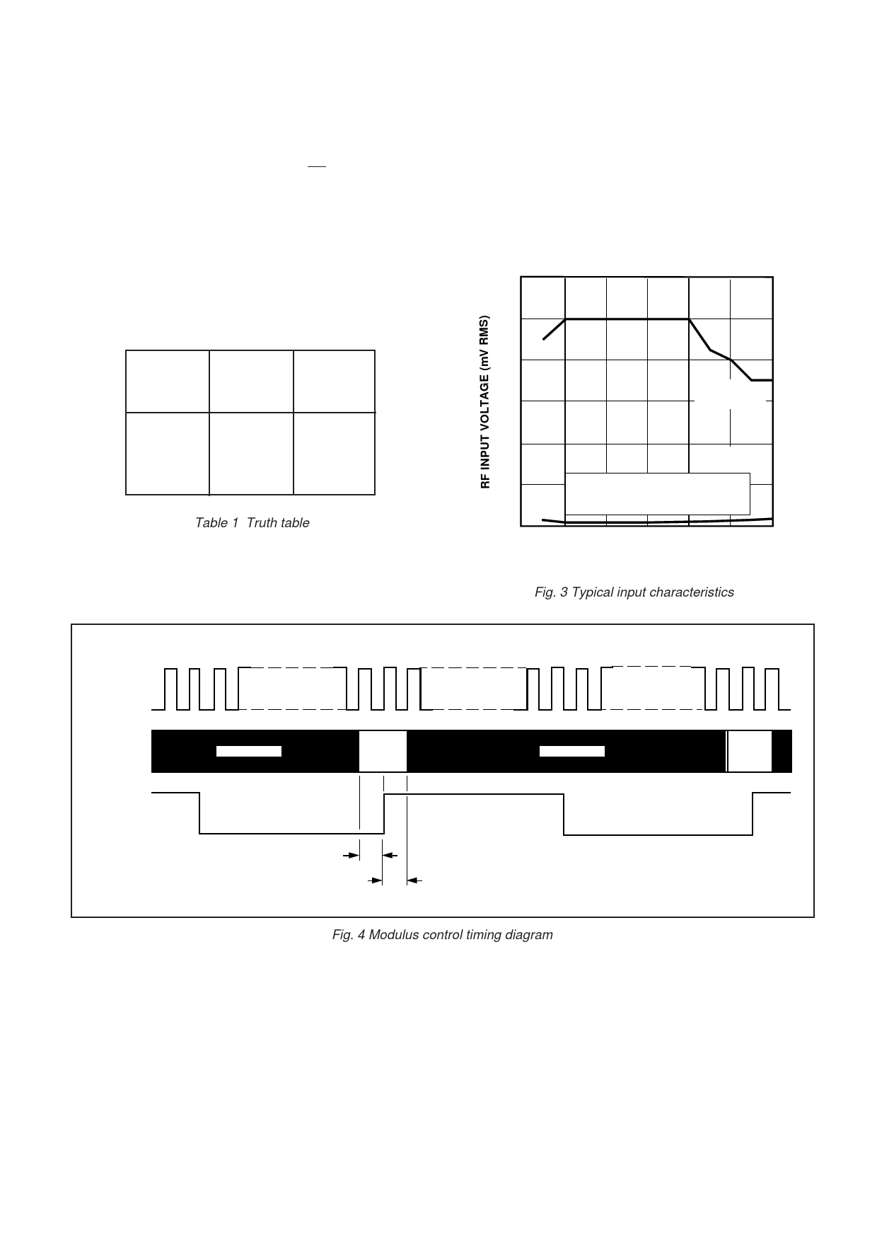
Modulus
Control 1
(Pin 3)
L
H
H
L
Modulus
Control 2
(Pin 6)
Division
Ratio
L
65
L
64
H
72
H
72
Table 1 Truth table
1000
800
TYPICAL
600
OVERLOAD
400
TYPICAL
SENSITIVITY
200
GUARANTEED*
OPERATING WINDOW
0
200 400 600 800 1000 1200
FREQUENCY (MHZ)
* Tested as specified in table of Electrical Characteristics
Fig. 3 Typical input characteristics
RF INPUT
CLOCK
MODULUS
CONTROL
INPUTS
OUTPUT
DON'T CARE
DON'T CARE
ts
th
32 or 36
Fig. 4 Modulus control timing diagram
32, 33 or 36
3
Share Link: 