T5743 데이터 시트보기 (PDF) - Atmel Corporation
부품명
상세내역
제조사
T5743 Datasheet PDF : 41 Pages
| |||
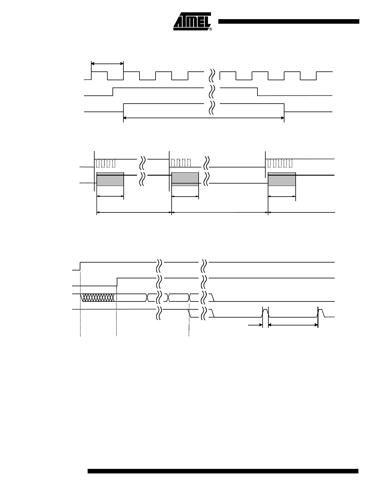
Figure 16. Synchronization of the Demodulator Output
T XClk
Clock bit-check
counter
Dem_out
Data_out (DATA)
tee
Figure 17. Debouncing of the Demodulator Output
Dem_out
Data_out (DATA)
tDATA_min
tee
tDATA_min
tee
tDATA_min
tee
Figure 18. Steady L State Limited DATA Output Pattern After Transmission
IC_ACTIVE
Bit check
Dem_out
Data_out (DATA)
Start-up mode
Bit-check mode
Receiving mode
tDATA_min
tDATA_L_max
After the end of a data transmission, the receiver remains active. Depending on the bit
Noise_Disable in the OPMODE register, the output signal at Pin DATA is high or ran-
dom noise pulses appear at Pin DATA (see section “Digital Noise Supression”). The
edge-to-edge time period tee of the majority of these noise pulses is equal or slightly
higher than TDATA_min.
16 T5743
4569A–RKE–12/02
Share Link: 