TS522 데이터 시트보기 (PDF) - STMicroelectronics
부품명
상세내역
제조사
TS522 Datasheet PDF : 5 Pages
| |||
TS522
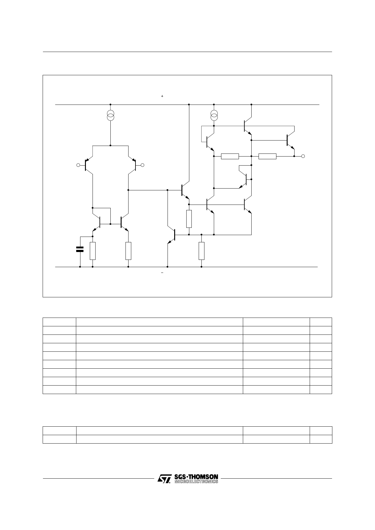
SCHEMATIC DIAGRAM (1/2 TS522)
VCC
Inverting
Input
Non-inverting
Input
Output
VCC
ABSOLUTE MAXIMUM RATINGS
Symbol
Parameter
Value
VCC
Supply Voltage
±18 or +36
Vid
Differential Input Voltage - (note 1)
±30
Vi
Input Voltage - (note 1)
±15
Output Short-Circuit Duration - (note 2)
Infinite
Toper
Operating Free-air Temperature Range
-40 to +105
Tj
Maximum Junction Temperature
+150
Tstg
Storage Temperature
-65 to +150
Ptot
Maximum Power Dissipation - (note 2)
500
Notes : 1. Either or both input voltages must not exceed the magnitude of VCC+ or VCC-
2. Power dissipation must be considered to ensure maximum junction temperature (Tj) is not exceeded
OPERATING CONDITIONS
Symbol
VCC
Supply Voltage
Parameter
Value
±2.5 to ±15
Unit
V
V
V
oC
oC
oC
mW
Unit
V
2/5
Share Link: 