TSA5512 데이터 시트보기 (PDF) - Philips Electronics
부품명
상세내역
제조사
TSA5512 Datasheet PDF : 20 Pages
| |||
Philips Semiconductors
1.3 GHz Bidirectional I2C-bus controlled synthesizer
Product specification
TSA5512
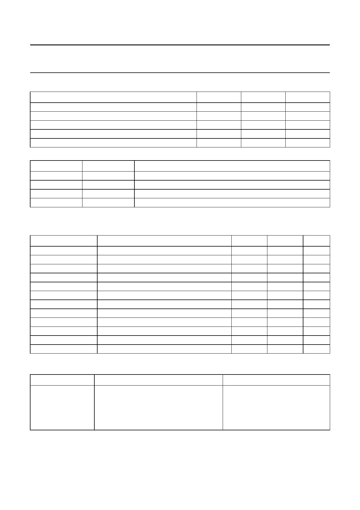
Table 3 ADC levels
VOLTAGE APPLIED ON THE PORT P6
0.6 VCC to 13.5 V
0.45 VCC to 0.6 VCC
0.3 VCC to 0.45 VCC
0.15 VCC to 0.3 VCC
0 to 0.15 VCC
A2
A1
A0
1
0
0
0
1
1
0
1
0
0
0
1
0
0
0
Table 4 Address selection
MA1
0
0
1
1
MA0
0
1
0
1
0 to 0.1 VCC
always valid
0.4 to 0.6 VCC
0.9 VCC to 13.5 V
VOLTAGE APPLIED ON PORT P3
LIMITING VALUES
In accordance with Absolute Maximum Rating System (IEC 134); all pin numbers refer to DIL18 version
VCC
V1
V2
V4
V5
V6-13
V15
V18
I6-13
I4
Tstg
Tj
SYMBOL
PARAMETER
supply voltage
charge-pump output voltage
crystal (Q1) input voltage
serial data input/output voltage
serial clock input voltage
P7 to P0 input/output voltage
prescaler input voltage
drive output voltage
P7 to P0 output current (open collector)
SDA output current (open collector)
IC storage temperature range
maximum junction temperature
MIN.
−0.3
−0.3
−0.3
−0.3
−0.3
−0.3
−0.3
−0.3
−1
−1
−40
−
MAX.
6
VCC
VCC
6
6
+16
VCC
VCC
15
5
+150
150
UNIT
V
V
V
V
V
V
V
V
mA
mA
°C
°C
THERMAL RESISTANCE
SYMBOL
Rth j-a
PARAMETER
from junction to ambient in free air
DIL18
SO16
SO20
SSOP20
THERMAL RESISTANCE
80 K/W
110 K/W
80 K/W
120 K/W
October 1992
9
Share Link: 