M74HC4852YRM13TR(2012) 데이터 시트보기 (PDF) - STMicroelectronics
부품명
상세내역
제조사
M74HC4852YRM13TR
(Rev.:2012)
(Rev.:2012)
STMicroelectronics
M74HC4852YRM13TR Datasheet PDF : 15 Pages
| |||
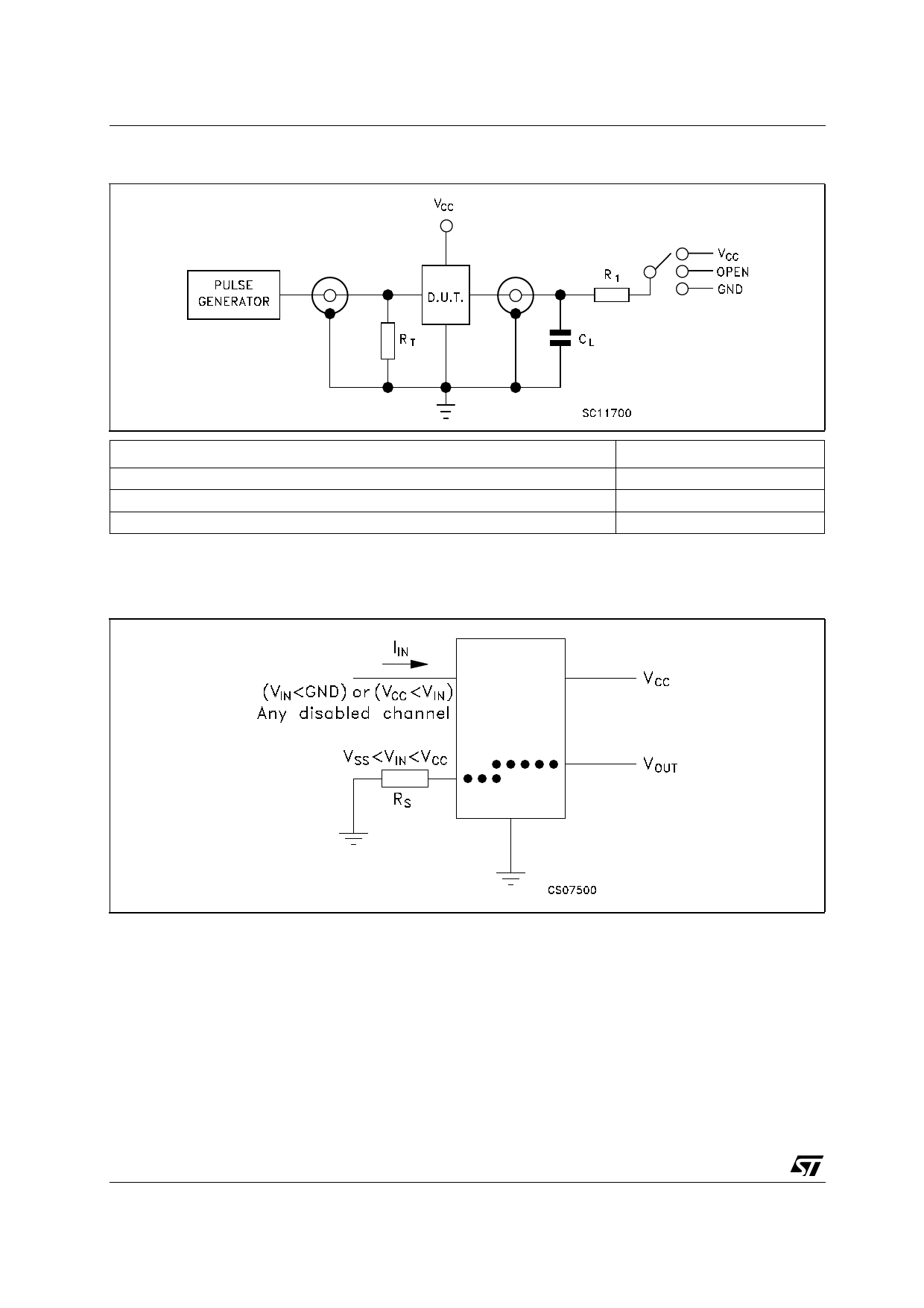
Absolute maximum ratings and operating conditions
M74HC4852
Table 6.
Symbol
DC specifications (continued)
Test condition
Parameter VCC
(V)
IIN
Control input
current
6.0
ICC
Quiescent
supply current
6.0
VIN = VCC or GND
VIN = VCC or GND
VIN (analog) = GND
Value
TA = 25 °C
Up to 85 °C Up to 125 °C Unit
Min. Typ. Max. Min. Max. Min. Max.
± 0.1
± 0.1
± 1 μA
2
20
40 μA
Table 7.
AC electrical characteristics (CL = 50 pF, input tr = tf = 6 ns)
Test condition
Value
Symbol Parameter VCC
(V)
tPHL,
tPLH
tPHL,
tPLH
tPHZ,
tPZH
tPLZ,,
tPZL
CIN
CIN
2.0
Propagation
3.0
delay time,
analog input to
3.3
analog output 4.5
6.0
2.0
Propagation
3.0
delay time
channel-select
3.3
to analog output 4.5
6.0
2.0
Enable disable 3.0
time, enable or
channel-select
3.3
to analog output 4.5
6.0
Input
capacitance
(digital pins)
Input
capacitance
(switches off,
any single
analog pins)
Test circuit 1
TA = 25 °C
Up to 85 °C Up to 125 °C Unit
Min. Typ. Max. Min. Max. Min. Max.
19.5 25
29
12 15.5
17.5
11 14.5
16.5
8.6 11.5
12.5
8 10
11
23 30
35
13.5 17.5
20
12.5 16.5
19
10 13
15
9.5 12.5
14.5
95
105
90
100
85
95
80
90
78
80
32
19.5
18.5 ns
13.5
12
40
23
22 ns
17
16.5
115
110
105 ns
100
80
3.5 10
10
10 pF
6.7 15
15
15 pF
6/15
Doc ID 8791 Rev 7
Share Link: 