SSM2402P 데이터 시트보기 (PDF) - Analog Devices
부품명
상세내역
제조사
SSM2402P Datasheet PDF : 12 Pages
| |||
SSM2402/SSM2412
ABSOLUTE MAXIMUM RATINGS
Operating Temperature Range . . . . . . . . . . . –40°C to +85°C
Operating Supply Voltage Range . . . . . . . . . . . . . . . . . ± 20 V
Analog Input Voltage Range
Continuous . . . . . . . . . . . . . . V– +3.5 V ≤ VA ≤ V+ –3.5 V
Maximum Current Through Switch . . . . . . . . . . . . . . 20 mA
Logic Input Voltage Range . . . . . . . . . . . . V+ Supply to –2 V
V+ Supply to Ground . . . . . . . . . . . . . . . . . . . . . . . . . . +36 V
V– Supply to Ground . . . . . . . . . . . . . . . . . . . . . . . . . . . –20 V
VA to V– Supply . . . . . . . . . . . . . . . . . . . . . . . . . . . . . . +36 V
Package Type
JA*
JC
Units
14-Pin Plastic DIP (P)
76
16-Pin SOL (S)
92
33
°C/W
27
°C/W
*θJA is specified for worst case mounting conditions, i.e., θJA is specified for device
in socket for P-DIP package; θJA is specified for device soldered to printed circuit
board for SOL package.
Model
SSM2402P
SSM2402S
SSM2412P
SSM2412S
ORDERING GUIDE
Temperature
Range
–40°C to +85°C
–40°C to +85°C
–40°C to +85°C
–40°C to +85°C
Package
Description
14-Pin Plastic DIP
16-Pin SOL
14-Pin Plastic DIP
16-Pin SOL
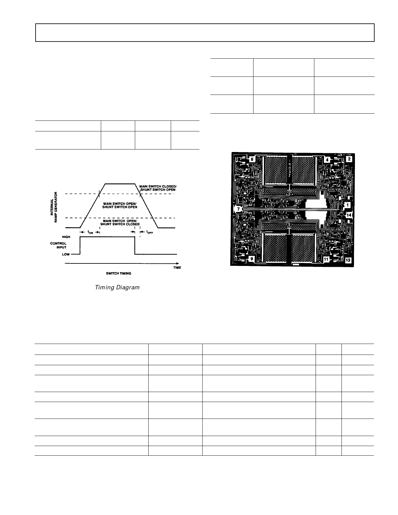
DICE CHARACTERISTICS
Die Size 0.105 × 0.097 Inch, 10,185 sq. mils
(2.667 × 2.464 mm, 6.57 sq. mm)
Timing Diagram
WAFER TEST LIMITS
Parameter
POSITIVE SUPPLY CURRENT
NEGATIVE SUPPLY CURRENT
GROUND CURRENT
Symbol
+ISY
–ISY
IGND
Conditions1
VIL = 0.8 V
VIL = 0.8 V
VIL = 0.8 V
Limit
7.5
6.0
1.5
Units
mA max
mA max
mA max
LOGIC INPUT CURRENT
ILOGIC
VIN = 0 V2
5.0
µA max
SWITCH ON RESISTANCE
RON
–14.2 V ≤ VA ≤ +14.2 V
IA = ± 10 mA, VIL = 2.0 V
85
Ω max
RON MATCH BETWEEN SWITCHES
RON MATCH
–14.2 V ≤ VA ≤ +14.2 V
IA = ± 10 mA, VIL = 2.0 V
5
% max
SWITCH ON LEAKAGE CURRENT
IS(ON)
–14.2 V ≤ VA ≤ +14.2 V, VIL = 2.0 V 1.0
µA max
SWITCH OFF LEAKAGE CURRENT
IS(OFF)
–14.2 V ≤ VA ≤ +14.2 V, VIL = 0.8 V 1.0
µA max
NOTES
1VIL = Logic Control Input; VA = Applied Analog Input Voltage; IA = Applied Analog Input Current.
2Worst Case Condition.
Electrical tests are performed at wafer probe to the limits shown. Due to variations in assembly methods and normal yield loss, yield after packaging is not
guaranteed for standard product dice. Consult factory to negotiate specifications based on dice lot qualifications through sample lot assembly and testing.
REV. A
–3–
Share Link: 