LT1167CS8 데이터 시트보기 (PDF) - Linear Technology
부품명
상세내역
제조사
LT1167CS8 Datasheet PDF : 20 Pages
| |||
APPLICATIO S I FOR ATIO
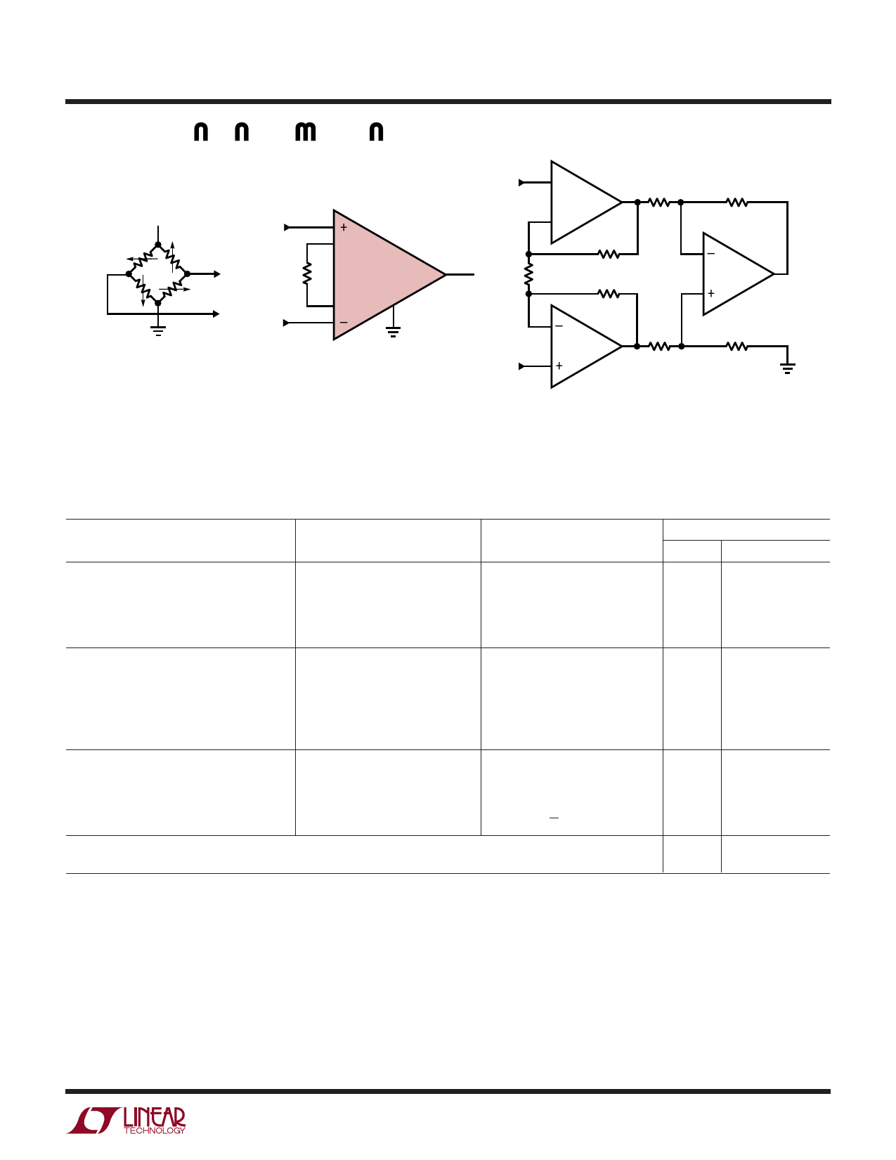
LT1167
10V
350Ω
350Ω
350Ω
350Ω
PRECISION BRIDGE TRANSDUCER
+
RG
499Ω
LT1167C
REF
–
LT1167 MONOLITHIC
INSTRUMENTATION AMPLIFIER
G = 100, RG = ±10ppm TC
SUPPLY CURRENT = 1.3mA MAX
+
1/4
10k*
LT1114A
–
10k**
202Ω**
10k**
10k*
–
1/4
+LT1114A
–
1/4
10k*
10k*
+LT1114A
“ROLL YOUR OWN” INST AMP, G = 100
* 0.02% RESISTOR MATCH, 3ppm/°C TRACKING
** DISCRETE 1% RESISTOR, ±100ppm/°C TC
100ppm TRACKING
SUPPLY CURRENT = 1.35mA FOR 3 AMPLIFIERS
1167 F06
Figure 6. “Roll Your Own” vs LT1167
Table 1. “Roll Your Own” vs LT1167 Error Budget
ERROR SOURCE
Absolute Accuracy at TA = 25°C
Input Offset Voltage, µV
Output Offset Voltage, µV
Input Offset Current, nA
CMR, dB
“ROLL YOUR OWN”’ CIRCUIT
LT1167C CIRCUIT CALCULATION CALCULATION
60µV/20mV
(300µV/100)/20mV
[(450pA)(350/2)Ω]/20mV
110dB→[(3.16ppm)(5V)]/20mV
100µV/20mV
[(60µV)(2)/100]/20mV
[(450pA)(350Ω)/2]/20mV
[(0.02% Match)(5V)]/20mV
Total Absolute Error
ERROR, ppm OF FULL SCALE
LT1167C “ROLL YOUR OWN”
3000
5000
150
60
4
4
790
500
3944
5564
Drift to 85°C
Gain Drift, ppm/°C
Input Offset Voltage Drift, µV/°C
Output Offset Voltage Drift, µV/°C
(50ppm + 10ppm)(60°C)
[(0.4µV/°C)(60°C)]/20mV
[6µV/°C)(60°C)]/100/20mV
(100ppm/°C Track)(60°C)
3600
[(1.6µV/°C)(60°C)]/20mV
1200
[(1.1µV/°C)(2)(60°C)]/100/20mV 180
Total Drift Error
4980
6000
4800
66
10866
Resolution
Gain Nonlinearity, ppm of Full Scale
Typ 0.1Hz to 10Hz Voltage Noise, µVP-P
15ppm
0.28µVP-P/20mV
G = 100, VS = ±15V
All errors are min/max and referred to input.
10ppm
(0.3µVP-P)(√ 2)/20mV
Total Resolution Error
Grand Total Error
15
10
14
21
29
31
8953
16461
Current Source
Figure 7 shows a simple, accurate, low power program-
mable current source. The differential voltage across Pins
2 and 3 is mirrored across RG. The voltage across RG is
amplified and applied across RX, defining the output
current. The 50µA bias current flowing from Pin 5 is
buffered by the LT1464 JFET operational amplifier. This
has the effect of improving the resolution of the current
source to 3pA, which is the maximum IB of the LT1464A.
Replacing RG with a programmable resistor greatly
increases the range of available output currents.
15
Share Link: 