STA-6033 데이터 시트보기 (PDF) - Sirenza Microdevices => RFMD
부품명
상세내역
제조사
STA-6033 Datasheet PDF : 8 Pages
| |||
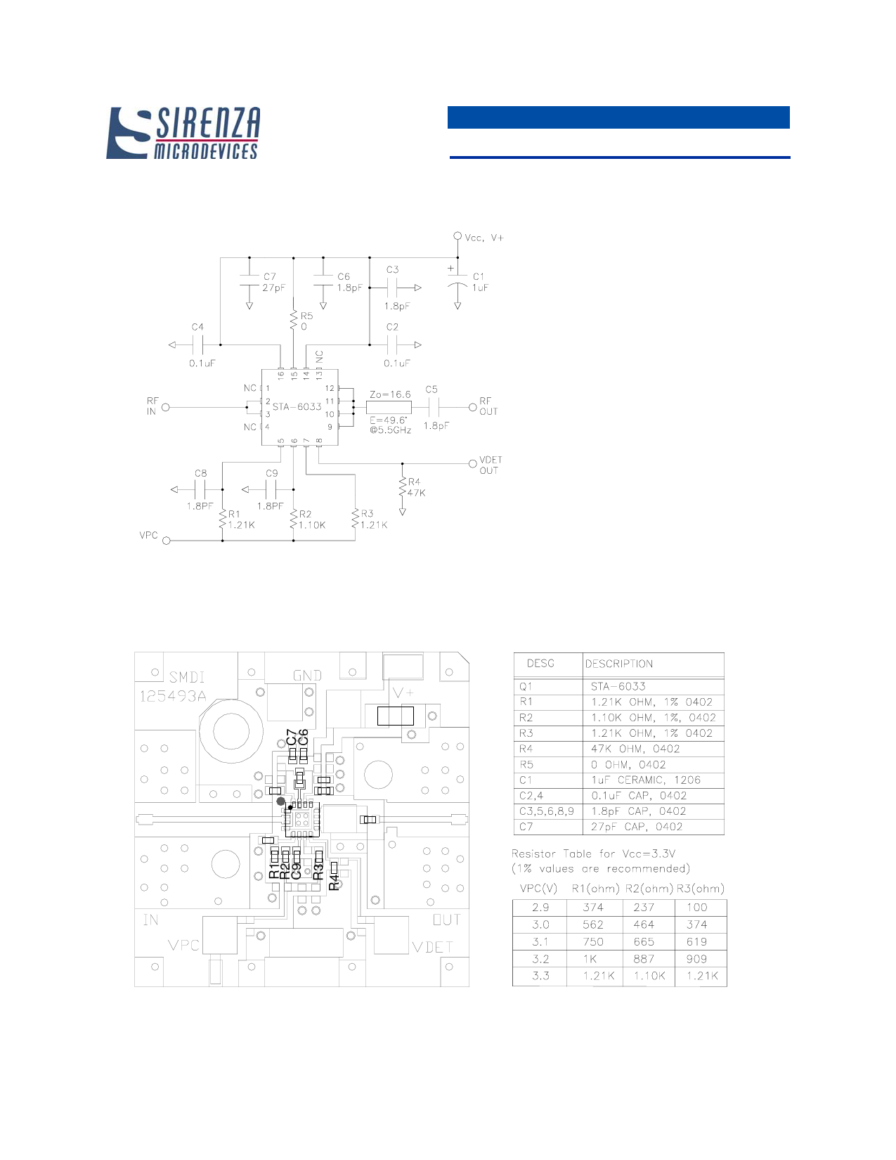
STA-6033 4.9-5.9 GHz Power Amp
4.9 - 5.9 GHz Evaluation Board Schematic For Vcc = Vpc = V+ = 3.3V Supply
Notes:
R5 (0 ohm jumper) is required for parasitic
inductance (~0.4nH).
R4 simulates external circuit loading to
ground. Recommended load range is 47K-
100K ohms.
Pins 1,4,9,12,13 are unwired (N/C) inside
the package. Refer to page 2 for detailed
pin descriptions. Some of these pins are
wired to adjacent pins or grounded as
shown in the application circuit. This is to
maintain consistency with the evaluation
board layout shown below. It is recom-
mended to use this layout and wiring to
achieve the specified performance.
To prevent potential damage, do not apply
voltage to the Vpc pin that is +1V greater
than voltage applied to pin 16 (Vbias/Vcc)
unless Vpc supply current capability is less
than 10 mA.
See table below for other Vpc logic level
resistor values.
4.9 - 5.9 GHz Evaluation Board Layout For Vcc = Vpc = V+ = 3.3V Supply
- Board material GETEK, 10mil thick, Dk=3.9, 2 oz. copper finish
C1
R5
C4
Q1
C8
C3
C2
C5
303 South Technology Court Broomfield, CO 80021
Phone: (800) SMI-MMIC
7
http://www.sirenza.com
EDS-103643 Rev F
Share Link: 