54405IVZ 데이터 시트보기 (PDF) - Intersil
부품명
상세내역
제조사
54405IVZ Datasheet PDF : 19 Pages
| |||
ISL54405
Electrical Specifications - 3.3V Supply Test Conditions: VDD = +3.0V to +3.6V, GND = 0V, VDIR_SEL = VAC/DC = GND,
V5V_SUPPLY = Float, VSIGNAL = 2VRMS, RLOAD = 20kΩ, f = 1kHz,
VSELH = VMUTEH = 1.4V, VSELL = VMUTEL = 0.5V, CAP_SS = 0.1µF, (Note 8),
Unless Otherwise Specified. (Continued)
PARAMETER
TEST CONDITIONS
TEM
SUPPL P
MIN
MAX
Y
(°C) (Notes 9, 10) TYP (Notes 9, 10) UNITS
Positive Supply Current, I+ VDD = +3.6V, VMUTE = 0V, VSEL = 0V or VDD
3.6V 25
-
Full
-
54
65
μA
59
-
μA
VDD = +3.6V, VMUTE = VDD, VSEL = 0V or VDD
3.6V 25
-
3.6V Full
-
14
18
μA
15
-
μA
VDD = +3.6V, VMUTE = 0V, VSEL = 1.8V
3.6V 25
-
3.6V Full
-
55
65
μA
58
-
μA
DIGITAL INPUT CHARACTERISTICS
Input Voltage Low, VSELL,
VMUTEL
3.3V, Full
-
5V
-
0.5
V
Input Voltage High, VSELH,
VMUTEH
3.3V, Full
1.4
-
5V
-
V
Input Current, ISELH, ISELL VDD = 3.6V, VMUTE = 0V, VSEL = 0V or VDD
3.6V Full
-0.5
0.01
0.5
µA
Input Current, IAC/DCL,
IDIR_SELL
VDD = 3.6V, VAC/DC, VDIR_SEL = 0V,
VMUTE = Float, VSEL = VDD
3.6V Full
-1.3
-0.7
0.3
µA
Input Current, IAC/DCH,
IDIR_SELH
VDD = 3.6V, VAC/DC, VDIR_SEL = VDD,
VMUTE = 0V, VSEL = 0V
3.6V Full
-0.5
0.01
0.5
µA
Input Current, IMUTEL
VDD = 3.6V, VSEL = VDD, VMUTE = 0V
3.6V Full
-1.3
-0.7
0.3
µA
Input Current, IMUTEH
VDD = 3.6V, VSEL = 0V, VMUTE = VDD
3.6V Full
-0.5
0.01
0.5
µA
NOTES:
8. VIN = input voltage to perform proper function.
9. The algebraic convention, whereby the most negative value is a minimum and the most positive a maximum, is used in this data sheet.
10. Parameters with MIN and/or MAX limits are 100% tested at +25°C, unless otherwise specified. Temperature limits established by characterization
and are not production tested.
11. Flatness is defined as the difference between maximum and minimum value of ON-resistance at the specified analog signal voltage points.
12. Limits established by characterization and are not production tested.
13. rON matching between channels is calculated by subtracting the channel with the highest max rON value from the channel with lowest max rON
value.
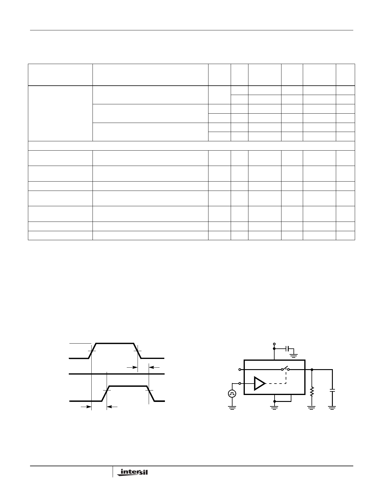
Test Circuits and Waveforms
VDD
LOGIC
INPUT
0V
50%
tOFF
tr < 20ns
tf < 20ns
SWITCH
INPUT
VLx OR VRx
SWITCH
OUTPUT 0V
VOUT
90%
tON
90%
Logic input waveform is inverted for switches that have the opposite
logic sense.
FIGURE 1A. MEASUREMENT POINTS
VDD C
SWITCH
INPUT
LOGIC
INPUT
Lx OR Rx
SEL
L or R
GND MUTE
VOUT
RL
CL
Repeat test for all switches. CL includes fixture and stray
capacitance.
VOUT
=
V(Lx or Rx)
---------R-----L---------
RL + rON
FIGURE 1B. TEST CIRCUIT
6
FN6699.1
June 5, 2008
Share Link: 