LT1614 데이터 시트보기 (PDF) - Linear Technology
부품명
상세내역
제조사
LT1614 Datasheet PDF : 16 Pages
| |||
LT1614
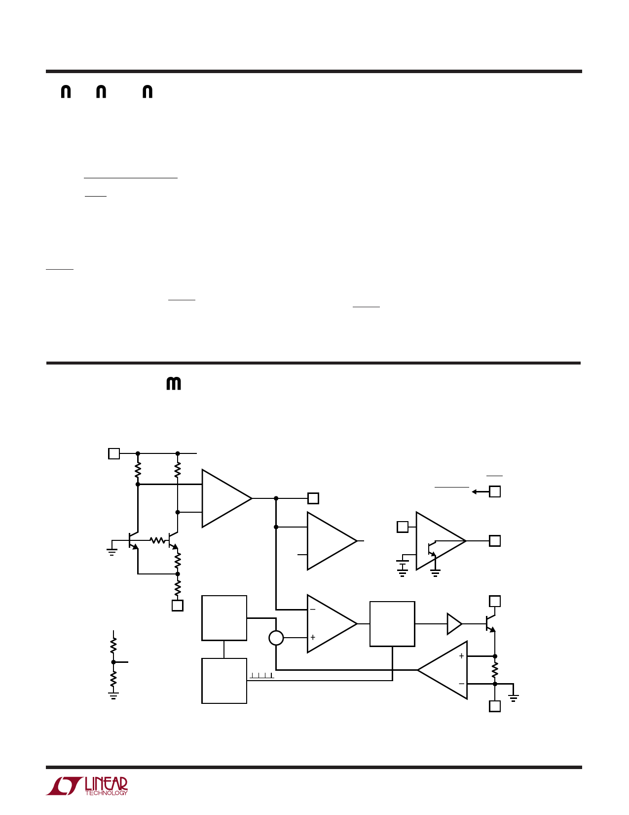
PIN FUNCTIONS
NFB (Pin 1): Negative Feedback Pin. Reference voltage is
– 1.24V. Connect resistive divider tap here. The sug-
gested value for R2 is 24.9k. Set R1 and R2 according to:
R1= | VOUT | – 1.24
1.24
R2
+
4.5
•
10–
6
VC (Pin 2): Compensation Pin for Error Amplifier. Con-
nect a series RC from this pin to ground. Typical values
are 100kΩ and 1nF. Minimize trace area at VC.
SHDN (Pin 3): Shutdown. Ground this pin to turn off
switcher. Must be tied to VIN (or higher voltage) to enable
switcher. Do not float the SHDN pin.
GND (Pin 4): Ground. Connect directly to local ground
plane.
SW (Pin 5): Switch Pin. Minimize trace area at this pin to
keep EMI down.
VIN (Pin 6): Supply Pin. Must have 1µF ceramic bypass
capacitor right at the pin, connected directly to ground.
LBI (Pin 7): Low-Battery Detector Input. 200mV refer-
ence. Voltage on LBI must stay between ground and
700mV. Float this pin if not used.
LBO (Pin 8): Low-Battery Detector Output. Open collec-
tor, can sink 10µA. A 1MΩ pull-up is recommended. Float
this pin if not used. The low-battery detector is disabled
when SHDN is low. LBO is high-Z in this state.
BLOCK DIAGRAM
VIN
6
R5
40k
Q1
VOUT
R1
(EXTERNAL)
NFB
R2
(EXTERNAL)
VIN
R6
40k
+
gm
–
ERROR
AMPLIFIER
Q2
A1
×10
R3
30k
R4
140k
1
NFB
RAMP
GENERATOR
600kHz
OSCILLATOR
VC
2
+
BIAS –
SHUTDOWN
LBI
7+
ENABLE
200mV
–
A4
COMPARATOR
–
FF
+
Σ
+
+
A2
R
Q
S
DRIVER
A=3
Figure 2. Block Diagram
SHDN
3
LBO
8
SW
5
Q3
0.15Ω
4
GND
1614 BD
5
Share Link: 