ADP3808JCPZ-RL 데이터 시트보기 (PDF) - ON Semiconductor
부품명
상세내역
제조사
ADP3808JCPZ-RL Datasheet PDF : 15 Pages
| |||
ADP3808A
VIN
C14
2.2uF
1/2 Q1
FD56990A
R13 C15 +
10R 22uF –
C9
L1
22uH +
1/2 Q1
FD56990A
C16
22uF
–
RCS
20mR
C13
22nF
R4
510R
RSS
10mR
SYSTEM
DC/DC
C1
2.2uF
R2
510R
3.3V
100nF
VCC BST DRV SW DRVL PGND
CSP CSM
SYSP SYSM
ISYS
LIMIT
DRVREG
5.25V
C10
0.1uF
EN
VREF + VREG
UVLO
BIAS
LOGIC
CONTROL
ADP3808A
AGND
BOOTSTRAPPED
SYNCHRONOUS
DRIVER
EN IN DRVLSD DRVLSD
–
+
+
–
+–
AMP1
VTH
–
gm1
+
AMP2
1V
SYSP
18.25V
OSCILLATOR
–
gm2
+
CHARGE
CURRENT
SETPOINT
BATTERY
VOLTAGE
ADJUST
3−/4−CELL
SELECTION
RT
COMP
150k
C8
0.22uF
R8
56R
C11
CELLSEL
LIMSET
EXTPWR
CSADJ
BAT
REFIN
BATADJ
BATTERY
12.6V/16.8V
3.3V
R9
R10
3.3V
R11
R12
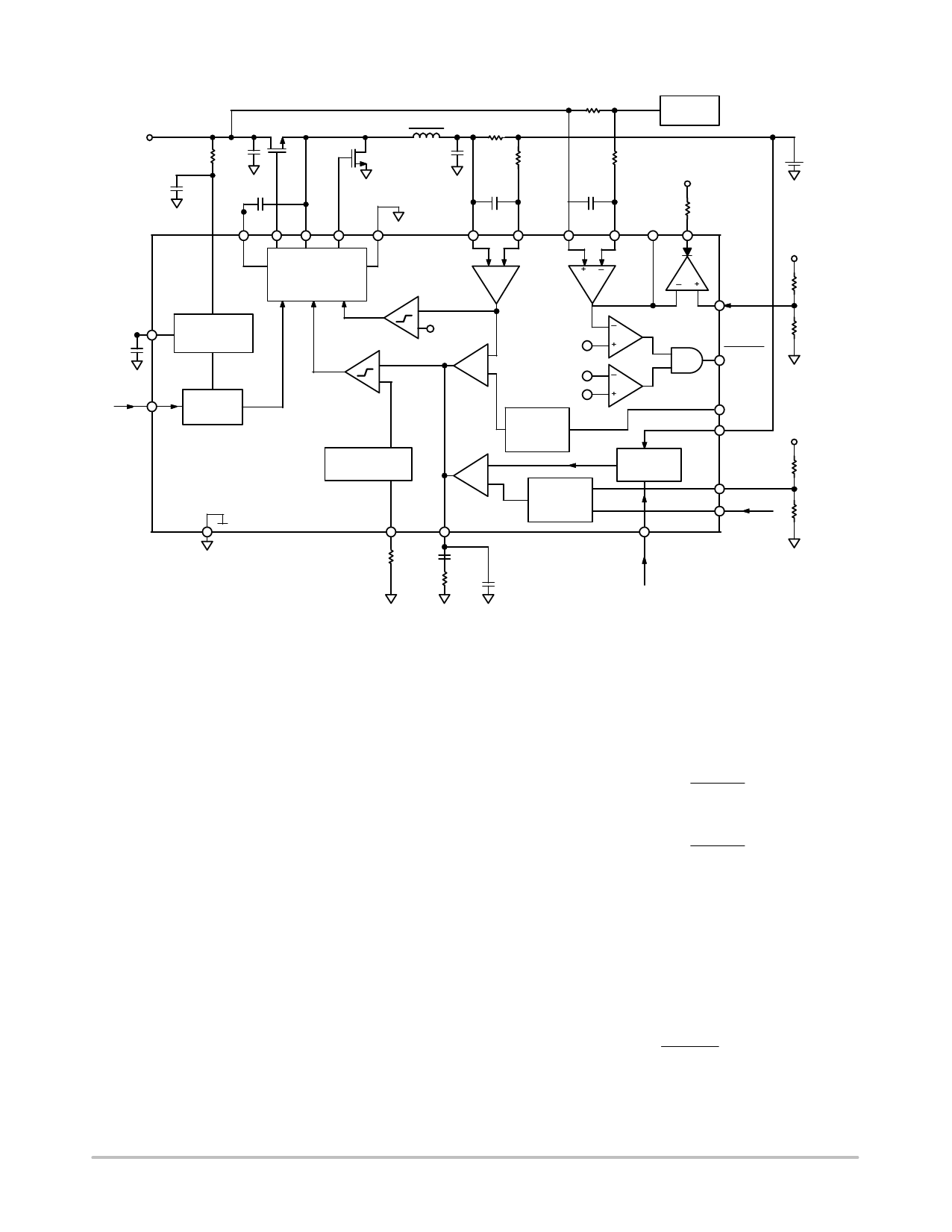
Figure 15. Typical Application Circuit
Final Battery Voltage Control
As the battery approaches its final voltage, the
ADP3808A switches from CC mode to CV mode. The
change is achieved by the common output node of gm1 and
gm2. Only one of the two outputs controls the voltage at the
COMP pin. Both amplifiers can only pulldown on COMP,
such that when either amplifier has a positive differential
input voltage, its output is not active. For example, when the
battery voltage, VBAT, is low, gm2 does not control VCOMP.
When the battery voltage reaches the desired final voltage,
gm2 takes control of the loop, and the charge current is
reduced.
Amplifier gm2 compares the battery voltage to a
programmable level set by pins BATADJ and REFIN. The
target battery voltage is dependent on the state of the
CELLSEL pin as CELLSEL sets the number of cells to be
charged. Pulling CELLSEL high sets the ADP3808A to
charge three cells. When CELLSEL is tied to ground, four
cells are selected. CELLSEL has a 2 mA pullup current as a
fail−safe to select three cells when it is left open.
The final battery voltage is programmable from 4.0 V to
4.5 V per cell. The programming voltage is applied to the
BATADJ pin and is ratioed to the REFIN pin. The battery
voltage VBAT is set according to Equation 2 and Equation 3.
For CELLSEL > 2 V:
VBAT
+
12
V ) 1.5
V
BATADJ
REFIN
(eq. 2)
For CELLSEL < 0.8 V:
VBAT
+
16
V ) 2.0
V
BATADJ
REFIN
(eq. 3)
Oscillator and PWM
The oscillator generates a triangle waveform between
1.0 V and 2.0 V, which is compared to the voltage at the
COMP pin, setting the duty cycle of the driver stage. When
VCOMP is below 1.0 V, the duty cycle is zero. Above 2.0 V,
the duty cycle reaches its maximum. The oscillator
frequency is set by the external resistor at the RT pin, ROSC,
and is given by Equation 4.
fOSC
+
41 109
ROSC
(eq. 4)
http://onsemi.com
11
Share Link: 