EL4095 데이터 시트보기 (PDF) - Intersil
부품명
상세내역
제조사
EL4095 Datasheet PDF : 19 Pages
| |||
EL4095
Absolute Maximum Ratings (TA = 25°C)
VS+ Supply Voltage . . . . . . . . . . . . . . . . . . . . . . . . . . . . . . . .+18V
VS Voltage between VS+ and VS- . . . . . . . . . . . . . . . . . . . .+33V
+VINA,Input Voltage . . . . . . . . . . . . . . . . . . . . . . . . . . . . . (VS-) -0.3V
+VINB . . . . . . . . . . . . . . . . . . . . . . . . . . . . . . . . . . . . to (VS+) +0.3V
IIN Current Into -VINA, -VINB . . . . . . . . . . . . . . . . . . . . . . . . 5mA
VGAIN Input Voltage . . . . . . . . . . . . . . . . . . . . . . . . . . . . . VGAIN ±5V
VGAIN Input Voltage . . . . . . . . . . . . . . . . . . . . . . . . . . . . . VS- to VS+
VFORCEInput Voltage . . . . . . . . . . . . . . . . . . . . . . . . . . . -1V to +6V
IOUT Output Current . . . . . . . . . . . . . . . . . . . . . . . . . . . . . . ±35mA
TA Operating Temperature Range . . . . . . . . . . . .-40°C to +85°C
TJ Operating Junction Temperature. . . . . . . . . . . 0°C to +150°C
TST Storage Temperature Range. . . . . . . . . . . . .-65°C to +150°C
Internal Power Dissipation . . . . . . . . . . . . . . . . . See Curves
CAUTION: Stresses above those listed in “Absolute Maximum Ratings” may cause permanent damage to the device. This is a stress only rating and operation of the
device at these or any other conditions above those indicated in the operational sections of this specification is not implied.
IMPORTANT NOTE: All parameters having Min/Max specifications are guaranteed. Typical values are for information purposes only. Unless otherwise noted, all tests
are at the specified temperature and are pulsed tests, therefore: TJ = TC = TA
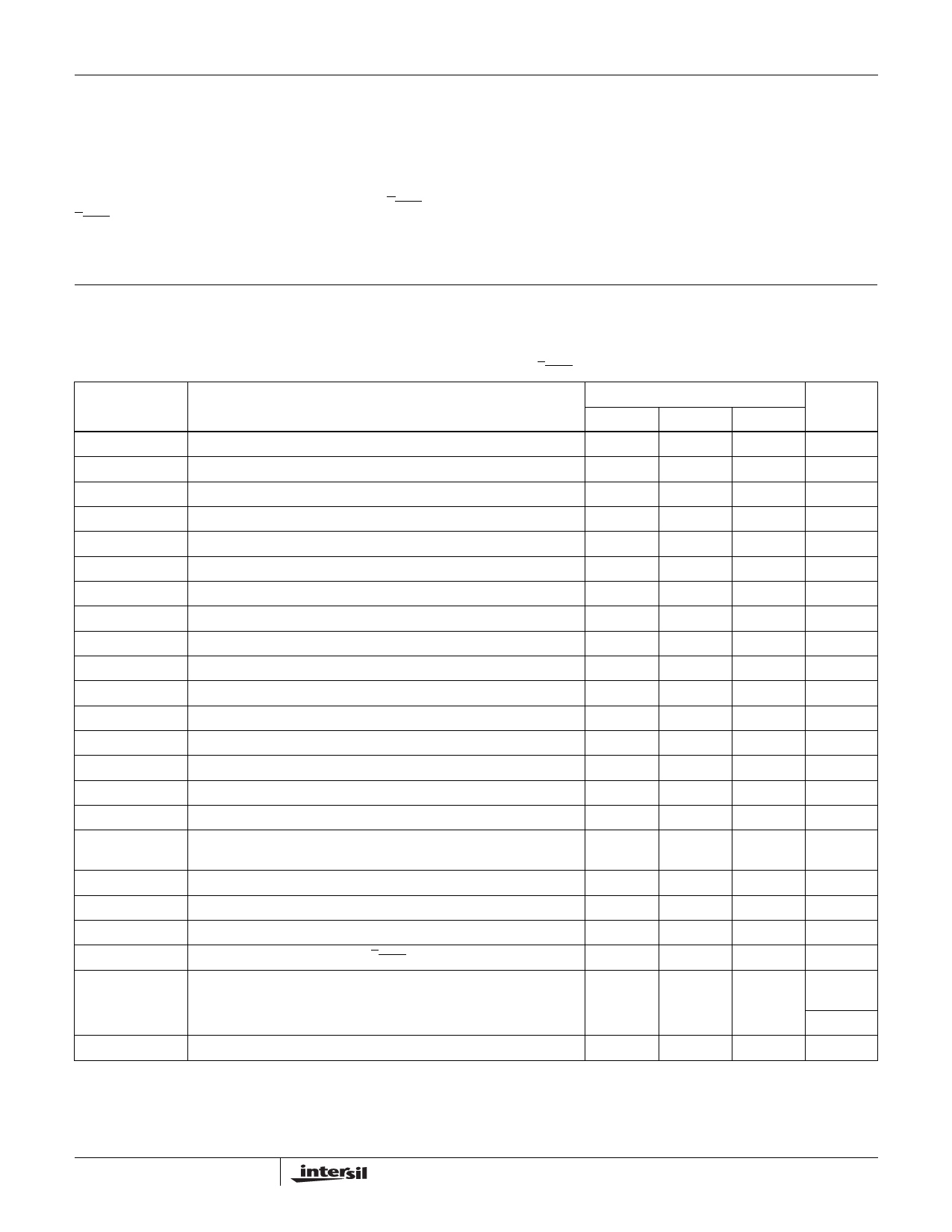
Open-Loop DC Electrical Specifications
VS = ±15V, TA = 25°C, VGAIN ground unless otherwise specified
LIMITS
PARAMETER
DESCRIPTION
MIN
TYP
MAX
VOS
IB+
IB-
CMRR
Input Offset Voltage
+VIN Input Bias Current
-VIN Input Bias Current
Common Mode Rejection
1.5
5
5
10
10
50
65
80
-CMRR
PSRR
-VIN Input Bias Current Common Mode Rejection
Power Supply Rejection Ratio
0.5
1.5
65
95
-IPSR
ROL
RIN-
VIN
VO
ISC
VIH
VIL
IFORCE, High
IFORCE, Low
Feedthrough,
Forced
-VIN Input Current Power Supply Rejection Ratio
Transimpedance
-VIN Input Resistance
+VIN Range
Output Voltage Swing
Output Short-Circuit Current
Input High Threshold at Force A or Force B Inputs
Input Low Threshold at Force A or Force B Inputs
Input Current of Force A or Force B, VFORCE = 5V
Input Current of Force A or Force B, VFORCE = 0V
Feedthrough of Deselected Input to Output,
Deselected Input at 100% Gain Control
0.2
(V-) + 3.5
(V-) +2
80
0.8
60
0.2
0.4
80
125
-440
75
2
(V+) -3.5
(V+) -2
160
2.0
-50
-650
VGAIN, 100%
VGAIN, 0%
NL, Gain
RIN, VG
NL, AV = 1
AV = 0.5
AV = 0.25
Minimum Voltage at VGAIN for 100% Gain
Maximum Voltage at VGAIN for 0% Gain
Gain Control Non-linearity, VIN = ±0.5V
Impedance between VGAIN and VGAIN
Signal Non-linearity, VIN = ±1V, VGAIN = 0.55V
Signal Non-linearity, VIN = ±1V, VGAIN = 0V
Signal Non-linearity, VIN = ±1V, VGAIN = -0.25V
0.45
-0.55
4.5
0.5
-0.5
2
5.5
<0.01
0.03
0.07
0.55
-0.45
4
6.5
0.4
IS
Supply Current
17
21
UNITS
mV
µA
µA
dB
µA/V
dB
µA/V
MΩ
Ω
V
V
mA
V
V
µA
µA
dB
V
V
%
kΩ
%
%
%
mA
2
Share Link: 