CY7C109V33-12ZC 데이터 시트보기 (PDF) - Cypress Semiconductor
부품명
상세내역
제조사
CY7C109V33-12ZC Datasheet PDF : 9 Pages
| |||
CY7C1009V33
CY7C109V33
Maximum Ratings
(Above which the useful life may be impaired. For user guide-
lines, not tested.)
Storage Temperature ................................. –65°C to +150°C
Ambient Temperature with
Power Applied ............................................. –55°C to +125°C
Supply Voltage on VCC to Relative GND[1] .... –0.5V to +7.0V
DC Voltage Applied to Outputs
in High Z State[1] .....................................–0.5V to VCC +0.5V
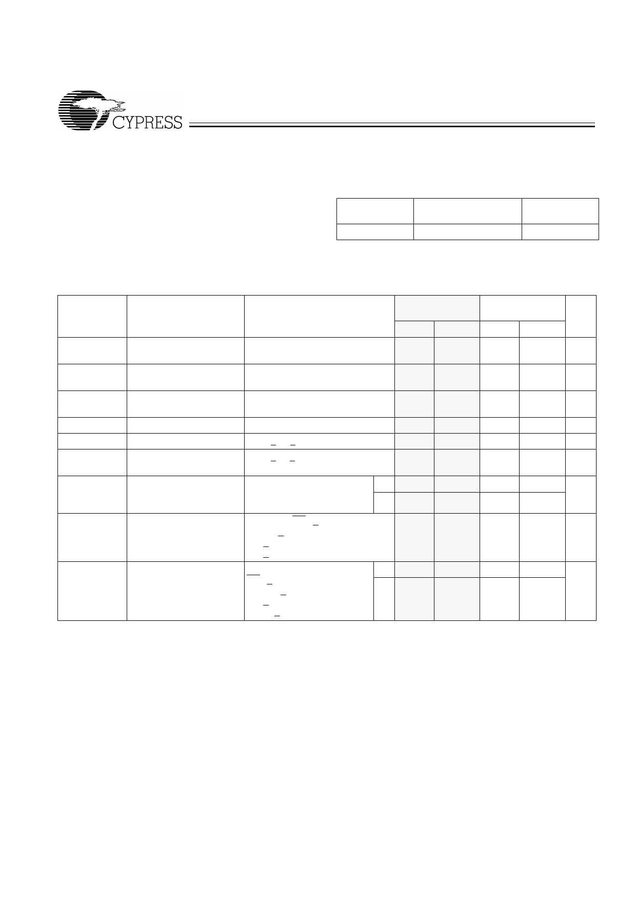
Electrical Characteristics Over the Operating Range
DC Input Voltage[1] ................................. –0.5V to VCC +0.5V
Current into Outputs (LOW)......................................... 20 mA
Operating Range
Range
Commercial
Ambient
Temperature[2]
0°C to +70°C
VCC
3.3V ± 300mV
Parameter
Description
VOH
Output HIGH Voltage
VOL
Output LOW Voltage
VIH
Input HIGH Voltage
Test Conditions
VCC = Min.,
IOH = –4.0 mA
VCC = Min.,
IOL = 8.0 mA
VIL
Input LOW Voltage[1]
IIX
Input Load Current
GND < VI < VCC
IOZ
Output Leakage
GND < VI < VCC,
Current
Output Disabled
ICC
VCC Operating
VCC = Max.,
Supply Current
IOUT = 0 mA,
f = fMAX = 1/tRC
L
ISB1
Automatic CE
Max. VCC, CE1 > VIH
Power-Down Current
or CE2 < VIL,
—TTL Inputs
VIN > VIH or
VIN < VIL, f = fMAX
ISB2
Automatic CE
Max. VCC,
Power-Down Current
—CMOS Inputs
CE1 > VCC – 0.3V,
or CE2 < 0.3V,
L
VIN > VCC – 0.3V,
or VIN < 0.3V, f=0
Shaded areas contain preliminary information.
Notes:
1. VIL (min.) = –2.0V for pulse durations of less than 20 ns.
2. TA is the case temperature.
7C109V33-12
7C1009V33-12
Min. Max.
2.4
7C1009V33-15
7C109V33–15
Min. Max. Unit
2.4
V
0.4
0.4
V
2.2
VCC
2.2
VCC
V
+ 0.3
+ 0.3
–0.3
0.8
–0.3
0.8
V
–1
+1
–1
+1
µA
–5
+5
–5
+5
µA
130
120 mA
90
80
25
20
mA
5
5
mA
2
2
2
Share Link: 