LC5540LD 데이터 시트보기 (PDF) - Sanken Electric co.,ltd.
부품명
상세내역
제조사
LC5540LD Datasheet PDF : 11 Pages
| |||
LC5540LD
Series
Single-Stage Power Factor Corrected
Off-Line Switching Regulators
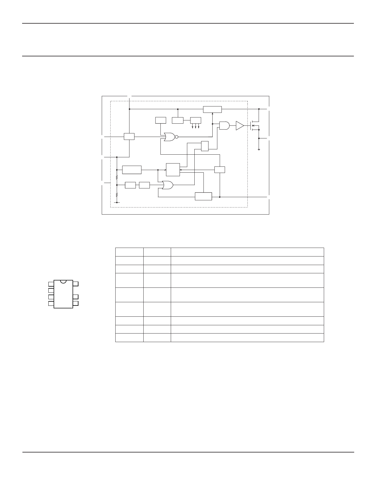
Functional Block Diagram
OVP ⑥
OCP ③
NF ⑤
VCC
②
OVP
TSD
UVLO
Control Part
START UP
Reg
Drv
Bias
S
RQ
Bottom
Detection
OCP LEB
Reg
OSC
OLP
Feedback
Control
⑧ D/ST
① S/GND
④ FB
Pin-out Diagram
S/GND 1
VCC 2
OCP 3
FB 4
8 D/ST
6 OVP
5 NF
Pin List Table
Number Name
1
S/GND
2
VCC
3
OCP
4
FB
5
NF
6
OVP
7
–
8
D/ST
Function
MOSFET source and GND pin for the Control Part
Supply voltage input and Overvoltage Protection (OVP) signal input
Overcurrent Protection (OCP), quasi-resonant signal input, and
Overvoltage Protection (OVP) signal input
Feedback phase-compensation input and Overload Protection
(OLP) signal input
No function; must be externally connected to S/GND pin with as
short a trace as possible, for stable operation of the IC
Overvoltage Protection (OVP) signal input
Pin removed
MOSFET drain pin and input of the startup current
LC5540LD-DS
8
SANKEN ELECTRIC CO., LTD.
Share Link: 