LD7750B 데이터 시트보기 (PDF) - Unspecified
부품명
상세내역
제조사
LD7750B Datasheet PDF : 19 Pages
| |||
LD7750B
Application Information
Operation Overview
As green power requirements become a trend and the
power saving gets more and more important for the
switching power supplies and switching adaptors, the
traditional PWM controllers are not able to support such
new requirements. Furthermore, the cost and size
limitations force PWM controllers to be more powerful by
integrating more functions and, thus, reducing the
external part counts. LD7750B is designed for such
application to provide an easy and cost effective solution.
Its detail features are described as below.
Internal High-Voltage Startup Circuit and
Under Voltage Lockout (UVLO)
The traditional circuits power the PWM controller on
through a startup resistor. It will constantly provide current
from a rectified voltage to the capacitor connected to Vcc
pin. Nevertheless, this startup resistor was usually of
larger resistance, and it therefore consumes more power
and requires more time to start up.
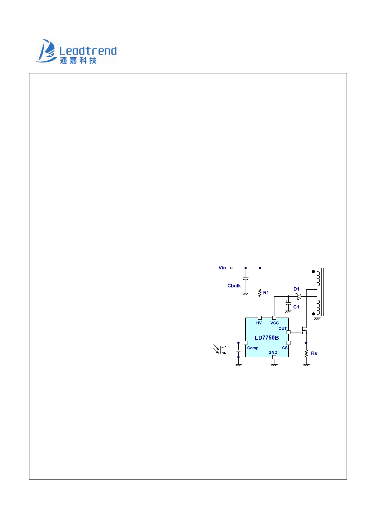
To achieve an optimized topology, as shown in Fig. 13,
The LD7750B is built in with high voltage startup circuit to
optimize the power saving. During the startup sequence, a
high-voltage current source sinks current from CBULK
capacitor to provide the startup current as well as to
charge the Vcc capacitor C1. During the initialization of
the startup, Vcc voltage is lower than the UVLO(off)
threshold thus the current source is on to supply a current
of 1mA. Meanwhile, as the Vcc current consumed by the
LD7750B is as low as 320μA thus most of the HV current
is utilized to charge the Vcc capacitor. By using such
configuration, the turn-on delay time will be almost the
same no matter what operation condition is, under
low-line or high-line.
When Vcc voltage reaches UVLO(on) threshold, the
LD7750B is powered on to start issuing the gate drive
signal, the high-voltage current source is then disabled,
and the Vcc supply current will be only provided from the
auxiliary winding of the transformer. Therefore, the
power loss on the startup circuit beyond the startup period
is minimized and the power saving is enhanced. In
general applications, a 39KΩ resistor is still recommended
to be placed in high voltage path to limit the current if
there is a negative voltage applying in any case.
An UVLO comparator is included to detect the voltage
over the VCC pin to ensure the supply voltage is high
enough to power on the LD7750B and in addition to drive
the power MOSFET as well. As shown in Fig. 14, a
hysteresis is provided to prevent the shutdown caused by
the voltage dip during startup.
Fig. 13
Leadtrend Technology Corporation
LD7750B-DS-01 OCT. 2011
9
www.leadtrend.com.tw
Share Link: 