MPSA92RLRAG 데이터 시트보기 (PDF) - ON Semiconductor
부품명
상세내역
제조사
MPSA92RLRAG Datasheet PDF : 5 Pages
| |||
MPSA92, MPSA93
High Voltage Transistors
PNP Silicon
Features
• Pb−Free Packages are Available*
MAXIMUM RATINGS
Rating
Symbol Value
Unit
Collector −Emitter Voltage
VCEO
Vdc
MPSA93
−200
MPSA92
−300
Collector −Base Voltage
VCBO
Vdc
MPSA93
−200
MPSA92
−300
Emitter −Base Voltage
Collector Current − Continuous
Total Device Dissipation
@ TA = 25°C
Derate above 25°C
VEBO
IC
PD
−5.0
−500
625
5.0
Vdc
mAdc
mW
mW/°C
Total Device Dissipation
@ TC = 25°C
Derate above 25°C
PD
1.5
W
12
mW/°C
Operating and Storage Junction
Temperature Range
TJ, Tstg
−55 to
°C
+150
THERMAL CHARACTERISTICS
Characteristic
Thermal Resistance,
Junction−to−Ambient
Symbol
RqJA
Max
200
Unit
°C/W
Thermal Resistance,
Junction−to−Case
RqJC
83.3
°C/W
Stresses exceeding Maximum Ratings may damage the device. Maximum
Ratings are stress ratings only. Functional operation above the Recommended
Operating Conditions is not implied. Extended exposure to stresses above the
Recommended Operating Conditions may affect device reliability.
http://onsemi.com
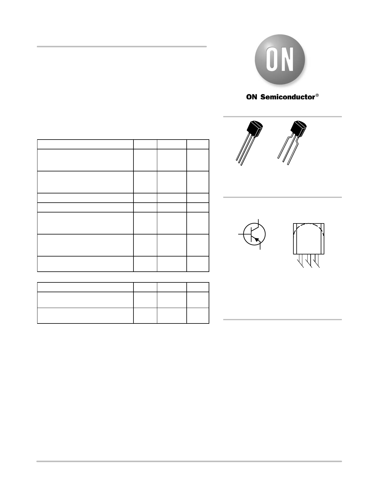
123
STRAIGHT LEAD
BULK PACK
TO−92
1
2
3
(TO−226AA)
CASE 29−11
BENT LEAD
TAPE & REEL
AMMO PACK
COLLECTOR
3
MARKING
DIAGRAM
2
BASE
1
EMITTER
MPS
A9x
AYWWG
G
x
= 2 or 3
A
= Assembly Location
Y
= Year
WW
= Work Week
G
= Pb−Free Package
(Note: Microdot may be in either location)
ORDERING INFORMATION
See detailed ordering and shipping information in the package
dimensions section on page 3 of this data sheet.
*For additional information on our Pb−Free strategy and soldering details, please
download the ON Semiconductor Soldering and Mounting Techniques
Reference Manual, SOLDERRM/D.
© Semiconductor Components Industries, LLC, 2010
1
July, 2010 − Rev. 6
Publication Order Number:
MPSA92/D
Share Link: 