LC74781 데이터 시트보기 (PDF) - SANYO -> Panasonic
부품명
상세내역
제조사
LC74781 Datasheet PDF : 16 Pages
| |||
LC74781, 74781M
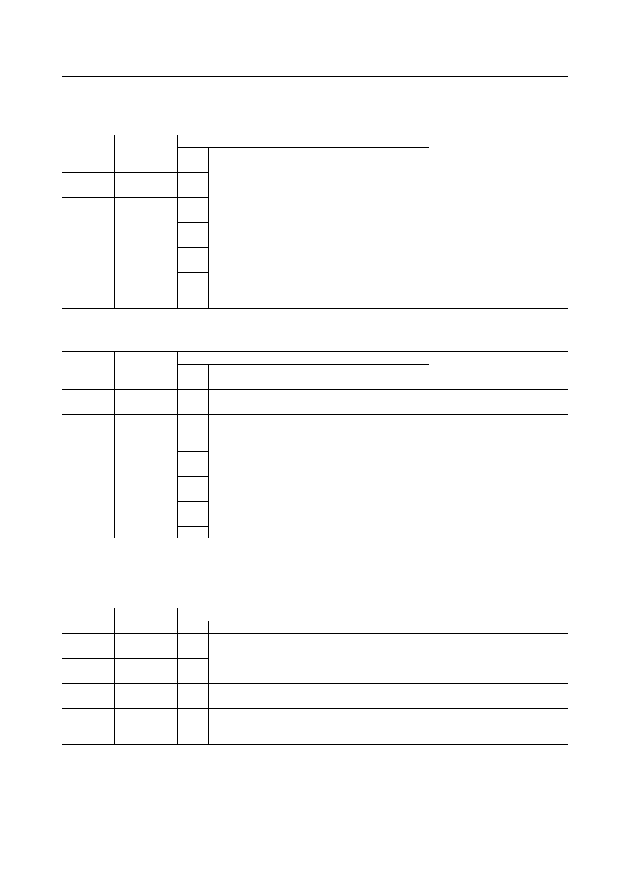
x COMMAND0 (Display memory write address setup command)
First byte
DA0 to DA7
7
6
5
4
3
2
1
0
Register name
—
—
—
—
V3
V2
V1
V0
State
1
0
0
0
0
1
0
1
0
1
0
1
Register content
Function
Command 0 identification code
Set the display memory write address.
Display memory address (0 to B hexadecimal)
Second byte
DA0 to DA7 Register name
State
Register content
Function
7
—
0 Second byte identification bit
6
—
0
5
—
0
0
4
H4
1
0
3
H3
1
0
2
H2
Display memory address (0 to 17 hexadecimal)
1
0
1
H1
1
0
0
H0
1
Note: The register states are all set to zero when the LC74781/M is reset with the RST pin.
COMMAND1 (Display character data write setup command)
First byte
DA0 to DA7
7
6
5
4
3
2
1
0
Register name
—
—
—
—
—
—
—
at
State
1
0
0
1
0
0
0
0
1
Register content
Function
Command 1 identification code
Set up display character data write.
Character attribute off
Character attribute on
Note
Note
Note
When this command is input, the
LC74781/M locks into the display
character data write mode until the CS
pin goes high.
No. 4988-8/16
Share Link: 