PS396CAI 데이터 시트보기 (PDF) - Pericom Semiconductor Corporation
부품명
상세내역
제조사
PS396CAI Datasheet PDF : 10 Pages
| |||
PS396
11223344556677889900112233445566778899001122334455667788990011221122334455667788990011223344556677889900112233445566778899001122112233445566778899001122334455P6677r88e99c0011is2233io4455n6677,8819900611-22C1122h3344a5566n77n8899e00l11,223314475566V7788A9900n1122a3344l55o66g7788M990011u2211l22t33i44p55l66e77x8899e00r1122
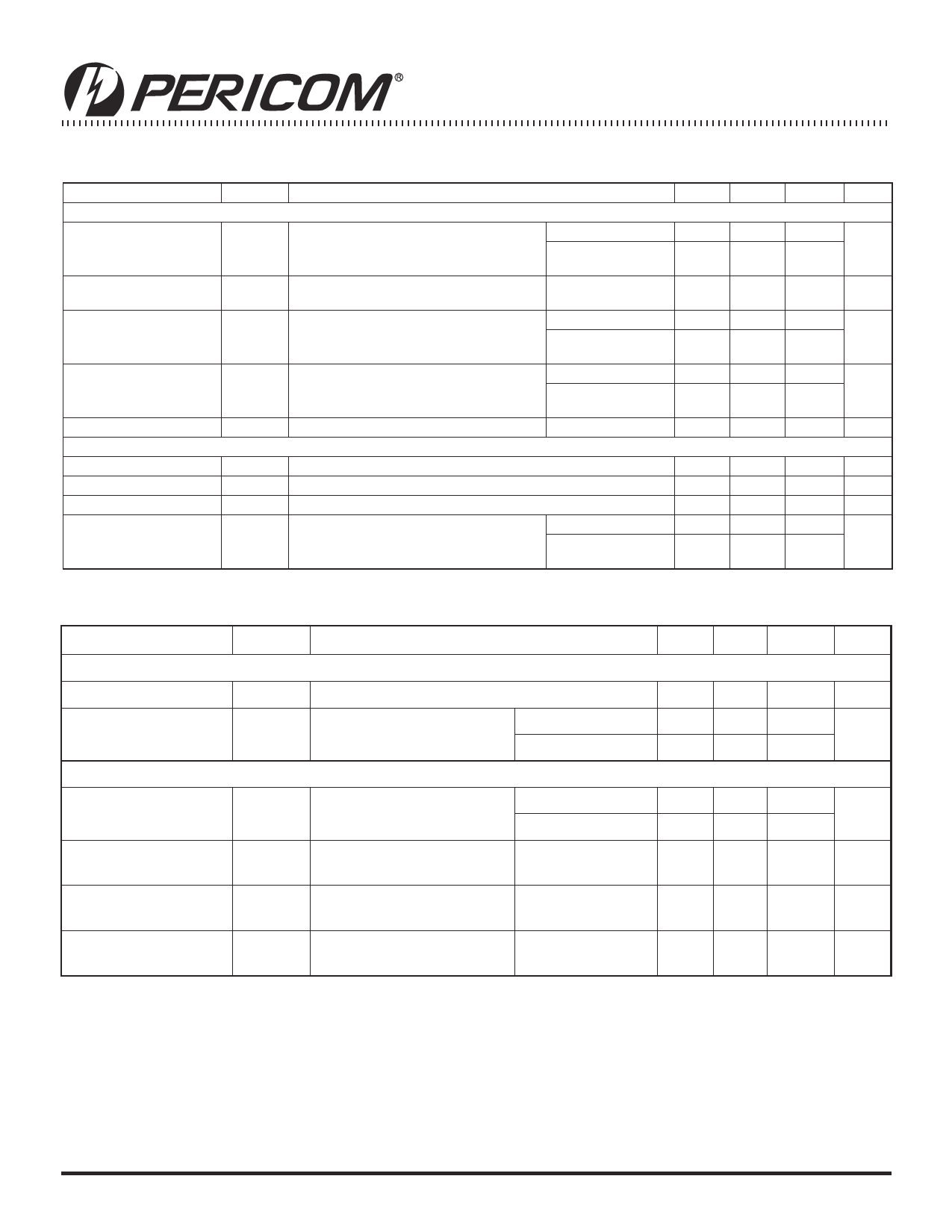
Electrical Characteristics — Single +5V Supply (continued)
(V+ = +5V ±10%, V– = 0V, GND = 0V, VAH = VENH = 2.4V, VAL = VENL = 0.8V, TA = TMin to TMax, unless otherwise noted.)
Parameter
Symbol
Conditions
Min.(2) Typ.(2) Max.(2)
Dynamic
Transition Time(3)
tTRANS VNO = 3V, Figure 2
TA = +25°C
TA = TMIN to
TMAX
105
245
350
Break-Before-Make
Time Delay
tOPEN (Note 3)
TA = +25°C
10
65
Enable Turn-On-Time(3)
tO N (EN )
TA = +25°C
TA = TMIN to
TMAX
125
200
275
Enable Turn-Off-Time(3)
Charge Injection (3)
tO F F (EN )
VCTE CL = 100pF, VNO = 0V, Figure 5
TA = +25°C
TA = TMIN to
TMAX
TA = +25°C
100
125
200
1.5
5
Supply
Power-Supply Range
V+
2.7
15
Positive Supply Current
I+
VEN = VA = 0V ,V+, V+ = 5.5V, V– = 0V
–1.0 0.06
1.0
Negative Supply Current
I–
VEN = VA = 0V ,V+, V+ = 5.5V, V– = 0V
–1.0 0.08
1.0
Ground Supply Current
IGND VEN = V+, 0V; V+, VA = 5.5V, V– = 0V
TA = +25°C
TA = TMIN to
TMAX
–1.0 0.08
1.0
–1.0
1.0
Units
ns
ns
ns
ns
pC
V
µA
µA
µA
Electrical Characteristics — Single +3.3V Supply
(V+ = 3.0V to 3.6V, GND = 0V, VINH = 2.4V, VINL = 0.8V, TA = TMin to TMax, unless otherwise noted.)
Parameter
Symbol
Conditions
Min.(2)
Typ.(2)
Max.(2)
Units
Switch
Analog Signal Range
On-Resistance
Dynamic
VANALOG (Note 3)
V–
V+
V
RON
INO = 1mA, VCOM = 1.5V,
V+ = 3V
TA = +25°C
TA = TMIN to TMAX
315 550
650
Ω
Transition Time(3)
Enable Turn-On-Time(3)
Enable Turn-Off-Time(3)
Charge Injection (3)
tTRANS
tON(EN)
tOFF(EN)
VCTE
VIN = 2.4V, VNO1 = 1.5V,
VNO8 = 0V, Figure 2
VINH = 2.4V, VINL = 0V,
VNO1 = 1.5V, Figure 3
VINH = 2.4V, VINL = 0V,
VNO1 = 1.5V, Figure 3
CL = 100pF, VGEN = 0V,
RGEN = 0 ohm Figure 6
TA = +25°C
TA = TMIN to TMAX
TA = +25°C
TA = +25°C
TA = +25°C
230 575
ns
750
260 500
ns
135 400
ns
1
5
pC
Notes:
2. The algebraic covention, where most negative value is a minimum and most positive value a maximum, is used in this data sheet.
3. Guaranteed by design
4. ∆RON = ∆RON(MAX) – RON(MIN)
5. Flatness is defined as the difference between the maximum and minimum value of on-resistance as measured over the specified
analog signal ranges. i.e., VNO = 3V to 0V and 0V to –3V.
6. Leakage parameters are guaranteed by desgin.
7. Worst-case isolation is on channel 4 because of its proximity to the COM pin. Off-isolation - 20log VCOM/VNO,
VCOM = output, VNO = input to off switch.
8. Leakage testing at single supply is guaranteed by correlation testing with dual supplies.
6
PS8443E
12/18/02
Share Link: 