ICS83026BGI-01LFT 데이터 시트보기 (PDF) - Integrated Circuit Systems
부품명
상세내역
제조사
ICS83026BGI-01LFT
Integrated Circuit Systems
ICS83026BGI-01LFT Datasheet PDF : 14 Pages
| |||
Integrated
Circuit
Systems, Inc.
ICS83026I-01
LOW SKEW, 1-TO-2
DIFFERENTIAL-TO-LVCMOS/LVTTL FANOUT BUFFER
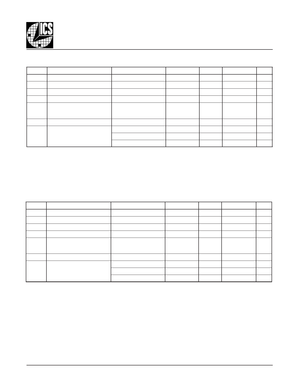
TABLE 4B. AC CHARACTERISTICS, VDD = 3.3V ± 5%, VDDO = 2.5V ± 5%, TA = -40°C TO 85°C
Symbol Parameter
Test Conditions
Minimum Typical Maximum
fMAX
tPD
tsk(o)
Output Frequency
Propagation Delay; NOTE 1
Output Skew; NOTE 2, 4
IJ 350MHz
350
1.5
2.0
2.6
15
tsk(pp) Part-to-Part Skew; NOTE 3, 4
750
Buffer Additive Phase Jitter,
tjit
RMS, refer to Additive Phase
0.03
Jitter Section
tR / tF
Output Rise/Fall Time
20% to 80%
150
800
IJ 66MHz
48
52
odc
Output Duty Cycle
67MHz ≤ ƒ≤ 166MHz
46
54
167MHz ≤ ƒ≤ 350MHz
40
60
NOTE 1: Measured from the differential input crossing point to VDDO/2 of the output.
NOTE 2: Defined as skew between outputs at the same supply voltage and with equal load conditions.
Measured at VDDO/2.
NOTE 3: Defined as skew between outputs on different devices operating at the same supply voltages and with
equal load conditions. Using the same type of inputs on each device, the outputs are measured at VDDO/2.
NOTE 4: This parameter is defined in accordance with JEDEC Standard 65.
Units
MHz
ns
ps
ps
ps
ps
%
%
%
TABLE 4C. AC CHARACTERISTICS, VDD = 3.3V ± 5%, VDDO = 1.8V ± 5%, TA = -40°C TO 85°C
Symbol Parameter
Test Conditions
Minimum Typical Maximum
fMAX
tPD
tsk(o)
Output Frequency
Propagation Delay; NOTE 1
Output Skew; NOTE 2, 4
IJ 350MHz
350
1.9
2.5
3.1
15
tsk(pp) Part-to-Part Skew; NOTE 3, 4
600
Buffer Additive Phase Jitter,
tjit
RMS, refer to Additive Phase
0.03
Jitter Section
tR / tF
Output Rise/Fall Time
20% to 80%
200
900
IJ 66MHz
48
52
odc
Output Duty Cycle
67MHz ≤ ƒ≤ 166MHz
43
57
167MHz ≤ ƒ≤ 350MHz
40
60
NOTE 1: Measured from the differential input crossing point to VDDO/2 of the output.
NOTE 2: Defined as skew between outputs at the same supply voltage and with equal load conditions.
Measured at VDDO/2.
NOTE 3: Defined as skew between outputs on different devices operating at the same supply voltages and with
equal load conditions. Using the same type of inputs on each device, the outputs are measured at VDDO/2.
NOTE 4: This parameter is defined in accordance with JEDEC Standard 65.
Units
MHz
ns
ps
ps
ps
ps
%
%
%
83026BMI-01
www.icst.com/products/hiperclocks.html
5
REV. A JANUARY 16, 2006
Share Link: 