ZL2106ALCF 데이터 시트보기 (PDF) - Renesas Electronics
부품명
상세내역
제조사
ZL2106ALCF Datasheet PDF : 29 Pages
| |||
ZL2106
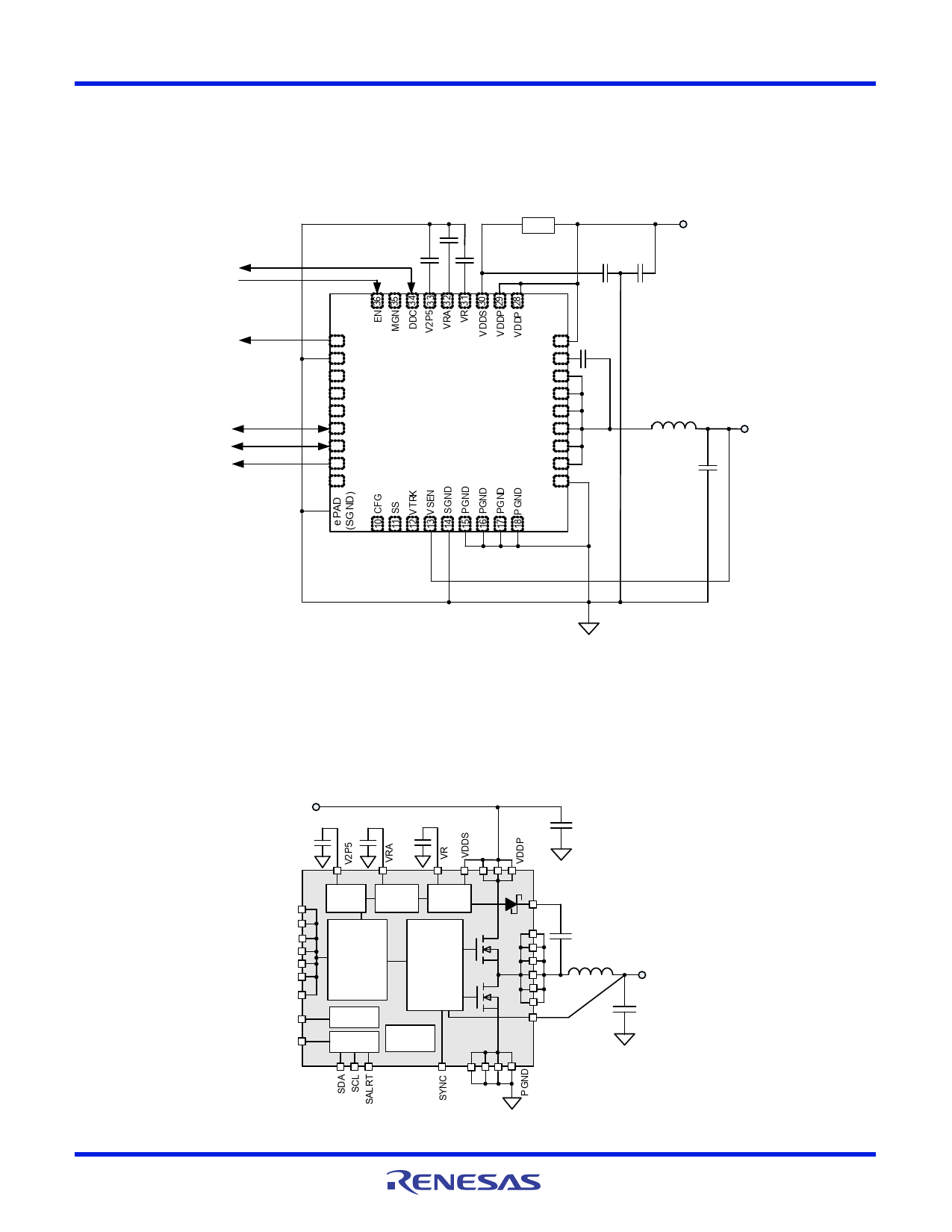
Typical Application Circuit
The following application circuit represents a typical
implementation of the ZL2106. For PMBus operation, it is
recommended to tie the enable pin (EN) to SGND.
C RA
4.7 µF
F.B.‡
DDC Bus†
ENABLE
C25
10 µF
CR
4.7µF
CDD
2.2 µF
CIN
100 µF
VIN
12V
PGOOD
I2C/
SMBus††
1 PG
2 DGND
3 SYNC
4 VSET
5 SA
6 SCL
7 SDA
8 SALRT
9 FC
ZL2106
VDDP 27
BST 26
SW 25
SW 24
SW 23
SW 22
SW 21
SW 20
PGND 19
CB
47nF
LOUT
2.2µH
C O UT
150 µF
VOUT
3.3V
Notes:
‡ Ferrite bead is optional for input noise suppression.
† The DDC bus pull-up resistance will vary based on the capacitive loading of the bus, including the number of devices
connected. The 10 k default value, assuming a maximum of 100 pF per device, provides the necessary 1 µs pull-up rise
time. Please refer to the Digital-DC Bus section for more details.
†† The I2C/SMBus pull -up resistance will vary based on the capacitive loading of the bus, including the number of devices
connected. Please refer to the I2C/SMBus specifications for more details.
FIGURE 2. 12V TO 3.3V/6A APPLICATION CIRCUIT (5ms SS DELAY, 5ms SS RAMP)
Block Diagram
VIN
EN
PG
MGN
VSET
CFG
SS
VTRK
DDC
SA
2.5V
LDO
5V
LDO
7V
LDO
Power
Mgmt
PWM
Control
&
Drivers
DDC Bus
SMBus
NVM
BST
SW
VSEN
VOUT
FN6852 Rev 6.00
February 20, 2013
FIGURE 3. BLOCK DIAGRAM
Page 3 of 29
Share Link: 