74LVC1G126(2010) 데이터 시트보기 (PDF) - Diodes Incorporated.
부품명
상세내역
제조사
74LVC1G126 Datasheet PDF : 14 Pages
| |||
74LVC1G126
SINGLE BUFFER GATE WITH 3-STATE OUTPUT
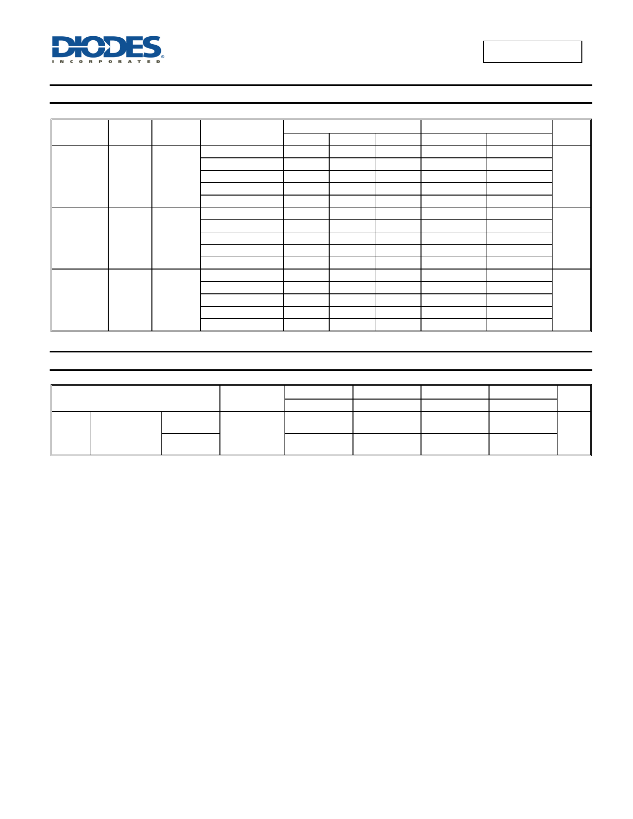
Electrical Characteristics (All typical values are at Vcc = 3.3V, TA = 25°C)
Over recommended free-air temperature range (unless otherwise noted)
Symbol
Parameter
Test Conditions
Vcc
Min
Typ. Max Unit
IOH = -100μA
IOH = -4mA
VOH
High Level Output
Voltage
IOH = -8mA
IOH = -16mA
IOH = -24mA
IOH = -32mA
IOH = 100μA
IOH = 4mA
High-level Input
VOL Voltage
IOH = 8mA
IOH = 16mA
IOH = 24mA
IOH = 32mA
II Input Current
VI = 5.5V or GND
IOFF
Power Down Leakage
Current
VI or VO = 5.5V
1.65V to 5.5V
1.65V
2.3V
3V
4.5V
1.65V to 5.5V
1.65V
2.3V
VCC – 0.1
1.2
1.9
2.4
2.3
3.8
3V
4.5V
0 to 5.5V
0
V
0.1
0.45
0.3
V
0.4
0.55
0.55
± 5 μA
± 10 μA
IOZ
OFF State Leakage
Current
VO = 0 to 5.5V
3.6V
10 μA
ICC Supply Current
ΔICC
Additional Supply
Current
VI = 5.5V of GND
IO = 0
One input at VCC –0.6V
Other inputs at VCC or
GND
1.65V to 5.5V
3V to 5.5V
10 μA
500 μA
Ci Input Capacitance
VI = VCC – or GND
SOT25
θJA
Thermal Resistance
Junction-to-Ambient
SOT353
DFN1410
SOT25
θJC
Thermal Resistance
Junction-to-Case
SOT353
DFN1410
3.3
(Note 5)
(Note 5)
(Note 5)
(Note 5)
(Note 5)
(Note 5)
4
pF
204
oC/W
371
oC/W
430
oC/W
52
oC/W
143
oC/W
190
oC/W
Notes: 5. Test condition for SOT25, SOT353, and DFN1410: Device mounted on FR-4 substrate PC board, 2oz copper, with minimum
recommended pad layout.
74LVC1G126
Document number: DS32103 Rev. 2 - 2
5 of 14
www.diodes.com
October 2010
© Diodes Incorporated
Share Link: 