ZXMP10A17GTA 데이터 시트보기 (PDF) - Unspecified
부품명
상세내역
제조사
ZXMP10A17GTA Datasheet PDF : 8 Pages
| |||
ZXMP10A17GTA
www.VBsemi.tw
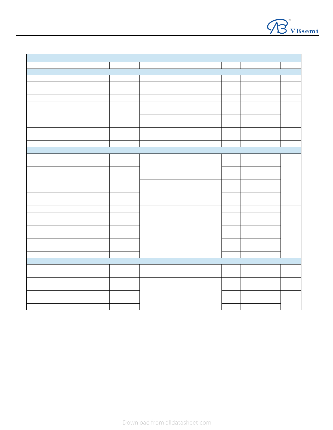
SPECIFICATIONS (TJ = 25 °C, unless otherwise noted)
Parameter
Symbol
Test Conditions
Static
Drain-Source Breakdown Voltage
VDS Temperature Coefficient
VGS(th) Temperature Coefficient
Gate-Source Threshold Voltage
Gate-Source Leakage
Zero Gate Voltage Drain Current
On-State Drain Currenta
Drain-Source On-State Resistancea
Forward Transconductancea
Dynamicb
VDS
VDS/TJ
VGS(th)/TJ
VGS(th)
IGSS
IDSS
ID(on)
RDS(on)
gfs
VGS = 0 V, ID = - 250 µA
ID = - 250 µA
VDS = VGS, ID = - 250 µA
VDS = 0 V, VGS = ± 20 V
VDS = - 100 V, VGS = 0 V
VDS = - 100 V, VGS = 0 V, TJ = 55 °C
VDS - 5 V, VGS = - 10 V
VGS = - 10 V, ID = - 3 A
VGS = - 6 V, ID = - 2 A
VDS = - 15 V, ID = 3 A
Input Capacitance
Output Capacitance
Reverse Transfer Capacitance
Total Gate Charge
Ciss
Coss
Crss
Qg
VDS = - 35 V, VGS = 0 V, f = 1 MHz
VDS = - 50 V, VGS = - 10 V, ID = - 3 A
Gate-Source Charge
Gate-Drain Charge
Gate Resistance
Turn-On Delay Time
Rise Time
Turn-Off DelayTime
Fall Time
Turn-On Delay Time
Rise Time
Turn-Off DelayTime
Fall Time
Drain-Source Body Diode Characteristics
Continuous Source-Drain Diode Current
Pulse Diode Forward Currenta
Body Diode Voltage
Body Diode Reverse Recovery Time
Body Diode Reverse Recovery Charge
Reverse Recovery Fall Time
Reverse Recovery Rise Time
Qgs
Qgd
Rg
td(on)
tr
td(off)
tf
td(on)
tr
td(off)
tf
IS
ISM
VSD
trr
Qrr
ta
tb
Notes:
a. Pulse test; pulse width 300 µs, duty cycle 2 %.
b. Guaranteed by design, not subject to production testing.
VDS = - 50 V, VGS = - 6 V, ID = - 3 A
f = 1 MHz
VDD = - 50 V, RL = 25
ID - 3 A, VGEN = - 6 V, Rg = 1
VDD = - 50 V, RL = 25
ID - 3 A, VGEN = - 10 V, Rg = 1
TC = 25 °C
IS = - 3 A
IF = - 3 A, dI/dt = 100 A/µs, TJ = 25 °C
Min.
- 100
-2
-8
Typ.
- 165
- 6.6
0.200
0.230
12
819
51
32
17.5
13.2
3.4
6.4
6.1
10
55
20
15
11
18
32
20
- 0.8
65
180
45
20
Max.
Unit
-4
± 100
-1
- 10
V
mV/°C
V
nA
µA
A
S
pF
32
25
nC
9.2
20
95
40
30
ns
18
32
58
35
- 13
A
- 15
- 1.2
V
90
ns
270
nC
ns
Stresses beyond those listed under “Absolute Maximum Ratings” may cause permanent damage to the device. These are stress ratings only, and functional operation
of the device at these or any other conditions beyond those indicated in the operational sections of the specifications is not implied. Exposure to absolute maximum
rating conditions for extended periods may affect device reliability.
E-mail:China@VBsemi TEL:86-755-83251052
2
Share Link: 