1EDF5673K 데이터 시트보기 (PDF) - Infineon Technologies
부품명
상세내역
제조사
1EDF5673K Datasheet PDF : 39 Pages
| |||
1EDF5673K, 1EDF5673F, 1EDS5663H
GaN gate driver
Isolation specifications
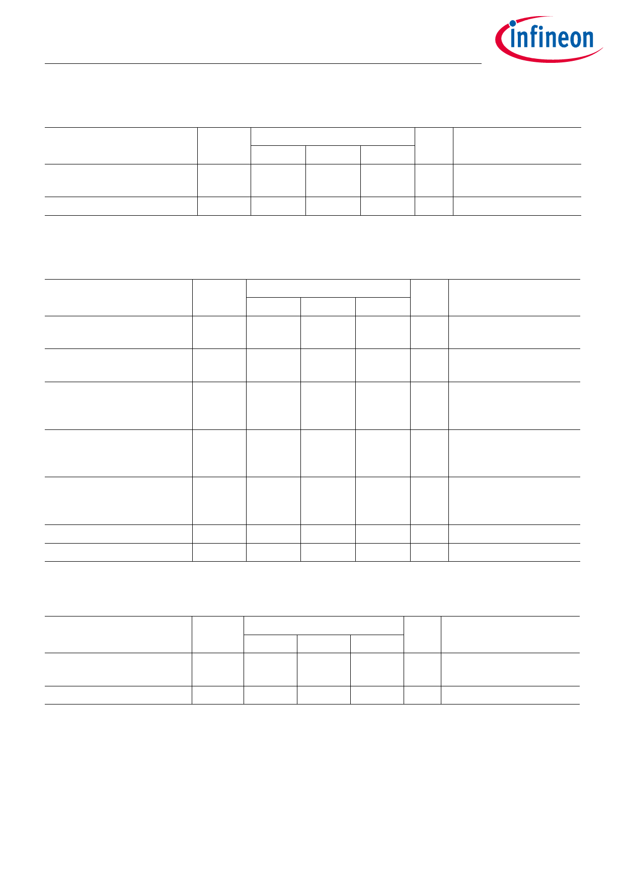
Table 12 Package characteristics (PG-TFLGA-13-1)
Parameter
Symbol
Values
Min.
Typ.
Comparative tracking Index of CTI
package mold
400
–
Material group
–
–
II
Max.
600
–
Unit Note or Test Condition
V
according to DIN EN
60112 (VDE 0303-11)
–
according to IEC 60112
7.1.2 Functional isolation in NB PG-DSO-16-11 package (1EDF5673F)
Table 13 Functional isolation input-to-output (NB PG-DSO-16-11)
Parameter
Symbol
Values
Unit Note or Test Condition
Min.
Typ.
Max.
Functional isolation test
VIO
voltage
1500
–
–
VDC impulse test > 10 ms,
sample tested
Maximum isolation working VIOWM
510
–
voltage
–
VRMS according to IEC 60664-1
(PD2; MG II)1)
Package clearance
CLR
–
4.0
– mm shortest distance over air,
from any input pin to any
output pin
Package creepage
CPG
–
4.0
– mm shortest distance over
surface, from any input
pin to any output pin
Common Mode Transient CMTI
200
Immunity
Capacitance input-to-output1) CIO
–
Resistance input-to-output1) RIO
–
1) verified by design, not tested in production
–
2
>1000
– V/ns according to VDE V0884-
10, static and dynamic
test
– pF –
– MΩ –
Table 14 Package characteristics (NB PG-DSO-16-11)
Parameter
Symbol
Values
Min.
Typ.
Comparative tracking Index of CTI
package mold
400
–
Material group
–
–
II
Max.
600
–
Unit Note or Test Condition
V
according to DIN EN 60112
(VDE 0303-11)
–
according to IEC 60112
Final datasheet
24
Rev. 2.3
2020-10-22
Share Link: 