LA7386 View Datasheet(PDF) - SANYO -> Panasonic
Part Name
Description
Manufacturer
LA7386 Datasheet PDF : 13 Pages
| |||
LA7386
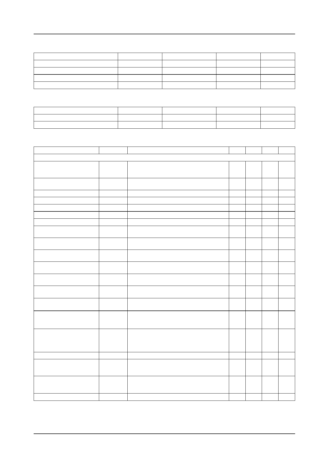
Maximum Ratings at Ta = 25°C
Parameter
Maximum supply voltage
Allowable power dissipation
Operating temperature
Storage temperature
Symbol
VCCmax
Pdmax
Topr
Tstg
Operating Conditions at Ta = 25°C
Conditions
Ta % 65°C
Ratings
Unit
7.0
V
1070
mW
–10 to +65
°C
–40 to +150
°C
Parameter
Recommended supply voltage
Operating supply voltage range
Symbol
VCC
VCCop
Conditions
Ratings
Unit
5.0
V
4.8 to 5.2
V
Operating Characteristics at Ta = 25°C, VCC = 5 V
Parameter
[REC Mode Y]
Current consumption REC
AGC adjustment
VCA control characteristics 1
VCA control characteristics 2
AGC adjustment voltage
AGC detection voltage
EE output level
AGC output 1
AGC output 2
AGC output 3
AGC output 4
Sync separation output level
Sync separation output pulse
width
Sync separation output leading
edge delay time
Sync separation threshold level
Sync tip level,
pedestal level,
white level measurement
(REC)
VCA detection voltage
Comb filter adjustment
Y-comb characteristics
C-comb characteristics
Symbol
ICCR
CAGC
VCA 1
VCA 2
VAGC
VAD
VEE
AGC 1
AGC 2
AGC 3
AGC 4
VSYR
PWSYR
∆ TSYR
THSYR
LVOR
VVCA
GY-Comb
GC-Comb
Conditions
When VCC = 5 V (when there is no signal),
measure sum of incoming currents at pins 29 and
24
VIN = 1.0 Vp-p video signal, use VR33 to adjust
T3 output to 0.5 Vp-p
Measure T3 output level when S9 is set to 2
Measure T3 output level when S9 is set to 4
Measure T33 DC voltage in above state
Measure T32 DC voltage in same manner
Measure T28A output level in same manner
VIN = 2.0 Vp-p video signal
Measure T3 output level
VIN = 0.5 Vp-p video signal
Measure T3 output level
VIN = 714 mVp-p LUMI, 572 mVp-p SYNC,
measure T3 SYNC level
VIN = 714 mVp-p LUMI, 143 mVp-p SYNC,
measure T3 SYNC level
VIN = 1.0 Vp-p video signal,
T26 output pulse peak value
VIN = 1.0 Vp-p video signal,
T26 output pulse width
VIN = 1.0 Vp-p video signal, measure delay time
of output SYNC versus input SYNC
Gradually attenuate the input level, measure input
level at point when output pulse width widens 1
µs or more beyond PWSYR
Measure electric potential for each of the T28
video output sync tip, pedestal, and white peak,
and assign the measured values to LSYN, LPED,
and LWHI, respectively
Measure T8 DC voltage
VIN = standard multiburst signal 1 Vp-p and S30
= off, adjust so that the 3.58 MHz component at
T21 is at a minimum
Measure the chroma level at T2 with a spectrum
analyzer, VIN = standard chroma noise test signal
1 Vp-p and S30 = off
VIN = white 50% + CW 3.0 MHz
min typ max Unit
95 120 145 mA
0.48 0.5 0.52 Vp-p
0.48 0.5 0.52 Vp-p
3.2 3.4 3.6
V
1.2 1.4 1.6
V
0.95 1.0 1.05 Vp-p
500 520 540 mVp-p
460 480 500 mVp-p
135 150 165 mVp-p
90 100 110 mVp-p
4.0 4.2 4.4 Vp-p
4.0
4.3 4.6
µs
0.8
1.0 1.2
µs
–18 –14 dB
2.80 2.95 3.10 V
–25 dB
–25 dB
Continued on next page.
No.5472 - 2/13
Share Link: 