HMP8154 View Datasheet(PDF) - Intersil
Part Name
Description
Manufacturer
HMP8154 Datasheet PDF : 34 Pages
| |||
HMP8154, HMP8156A
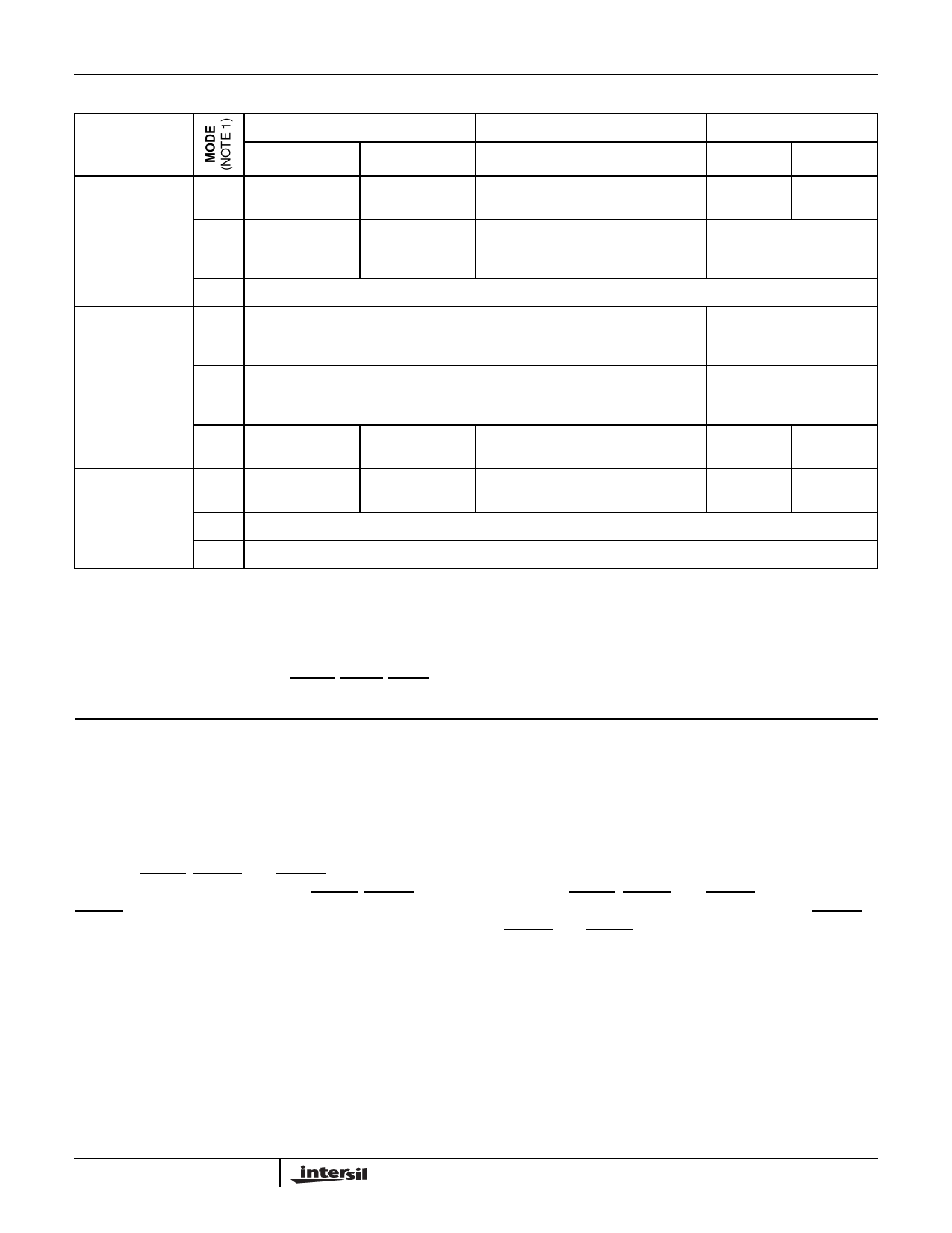
TABLE 5. PIXEL INPUT AND CONTROL SIGNAL I/O TIMING
INPUT PORT SAMPLING
VIDEO TIMING CONTROL (NOTE 2)
CLK FREQUENCY
INPUT FORMAT
PIXEL DATA OVERLAY DATA INPUT SAMPLE
OUTPUT ON
INPUT
OUTPUT
8-Bit YCbCr
Norm Every rising edge Same edge that
of CLK2
latches Y
Every rising edge Any rising edge of Ignored
of CLK2
CLK2
One-half
CLK2
2X Rising edge of
Same edge that
CLK2 when CLK is latches Y data
low.
Rising edge of
Rising edge of
CLK2 when CLK is CLK2 when CLK is
low.
high.
One-half CLK2
FF
Not Available
16-Bit YCbCr,
16-Bit RGB,
or
24-Bit RGB
Norm Rising edge of CLK2 when CLK is low
2X 2nd rising edge of CLK2 when CLK is low
Rising edge of
CLK2 when CLK is
high.
Either rising CLK2
edge when CLK is
high
One-half CLK2
One-fourth CLK2
FF Every rising edge Same edge that
of CLK2
latches Y
Every rising edge Any rising edge of Ignored
of CLK2
CLK2
One-half
CLK2
BT.656
Norm Every rising edge Same edge that
of CLK2
latches Y
Not Allowed
Any rising edge of Ignored
CLK2
One-half
CLK2
2X
Not Available
FF
Not Available
NOTES:
1. Encoder operating modes:
Norm = Full size input, Flicker filter disabled.
2X = SIF size input, Flicker filter disabled.
FF = Full size input, Flicker filter enabled.
(2X upscaling and flicker filtering are mutually exclusive.)
2. Video timing control signals include HSYNC, VSYNC, BLANK and FIELD. The sync and blanking I/O directions are independent; FIELD is always
an output.
Normal 8-Bit YCbCr Format
When 8-bit YCbCr format is selected and 2X upscaling or
flicker filtering is not enabled, the data is latched on each
rising edge of CLK2. The pixel data must be [Cb Y Cr Y’ Cb Y
Cr Y’ . . . ], with the first active data each scan line being Cb
data. Overlay data is latched when the Y input data is latched.
The pixel and overlay input timing is shown in Figure 1.
As inputs, BLANK, HSYNC, and VSYNC are latched on
each rising edge of CLK2. As outputs, BLANK, HSYNC, and
VSYNC are output following the rising edge of CLK2. If the
CLK pin is configured as an input, it is ignored. If configured
as an output, it is one-half the CLK2 frequency.
8-Bit YCbCr Format with 2X Upscaling
When 8-bit YCbCr format is selected and 2X upscaling is
enabled, the data is latched on the rising edge of CLK2 while
CLK is low. The pixel data must be [Cb Y Cr Y’ Cb Y Cr
Y’. . . ], with the first active data each scan line being Cb
data. Overlay data is latched on the rising edge of CLK2 that
latches Y pixel input data. The pixel and overlay input timing
is shown in Figure 2.
As inputs, BLANK, HSYNC, and VSYNC are latched on the
rising edge of CLK2 while CLK is low. As outputs, HSYNC,
VSYNC, and BLANK are output following the rising edge of
CLK2 while CLK is high. In this mode of operation, CLK is
one-half the CLK2 frequency.
6
4343.4
November 4, 2005
Share Link: 