MPSW01G(2010) View Datasheet(PDF) - ON Semiconductor
Part Name
Description
Manufacturer
MPSW01G Datasheet PDF : 4 Pages
| |||
MPSW01, MPSW01A
One Watt High Current
Transistors
NPN Silicon
Features
• Pb−Free Packages are Available*
MAXIMUM RATINGS
Rating
Collector −Emitter Voltage
Symbol
MPSW01
MPSW01A
VCEO
Value
30
40
Unit
Vdc
Collector −Base Voltage
VCBO
Vdc
MPSW01
40
MPSW01A
50
Emitter −Base Voltage
Collector Current − Continuous
Total Device Dissipation @ TA = 25°C
Derate above 25°C
VEBO
IC
PD
5.0
1000
1.0
8.0
Vdc
mAdc
W
mW/°C
Total Device Dissipation @ TC = 25°C
PD
2.5
W
Derate above 25°C
20
mW/°C
Operating and Storage Junction
Temperature Range
TJ, Tstg −55 to +150 °C
THERMAL CHARACTERISTICS
Characteristic
Symbol
Max
Unit
Thermal Resistance, Junction−to−Ambient RqJA
125
°C/W
Thermal Resistance, Junction−to−Case
RqJC
50
°C/W
Stresses exceeding Maximum Ratings may damage the device. Maximum
Ratings are stress ratings only. Functional operation above the Recommended
Operating Conditions is not implied. Extended exposure to stresses above the
Recommended Operating Conditions may affect device reliability.
http://onsemi.com
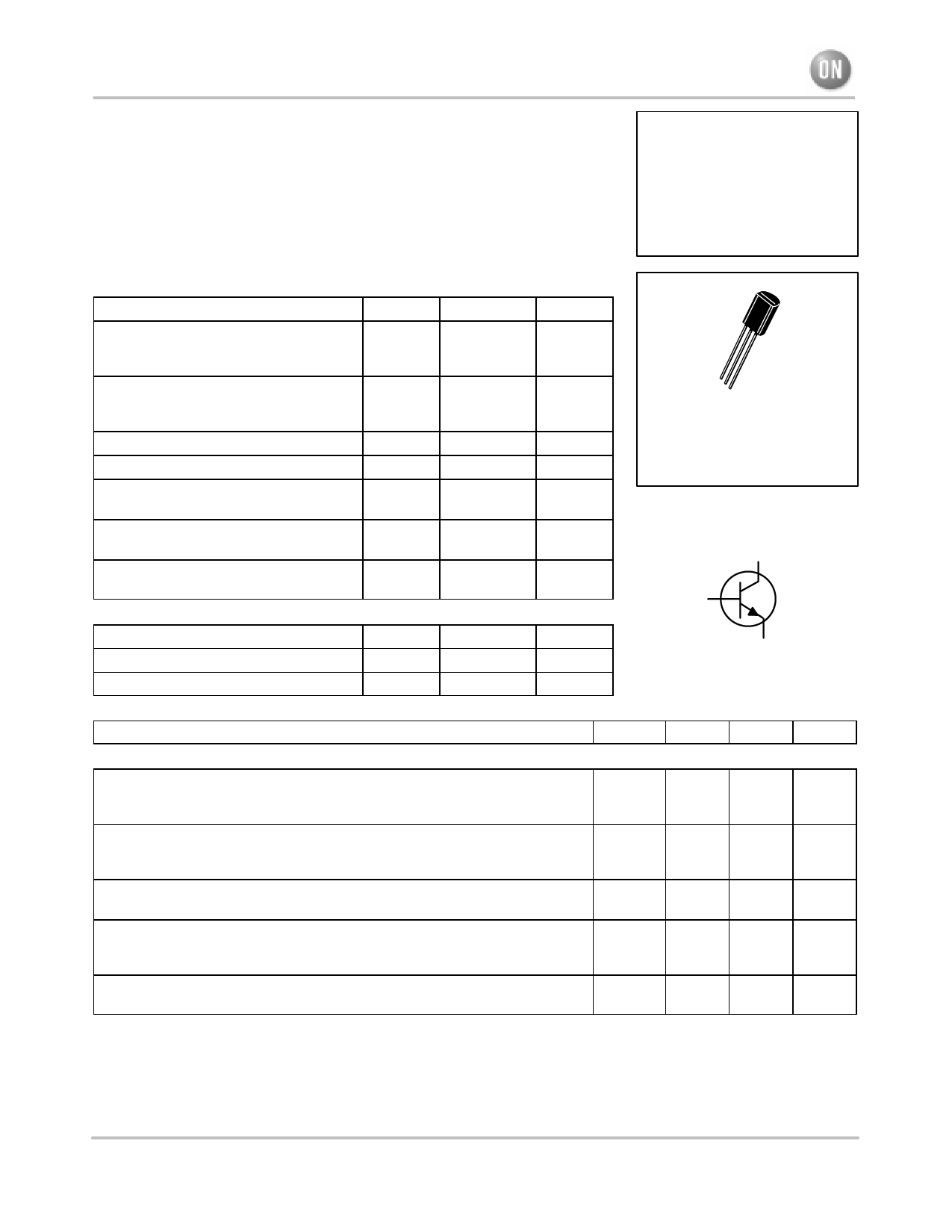
COLLECTOR
3
2
BASE
1
EMITTER
TO−92 (TO−226AE)
CASE 29−10
STYLE 1
MARKING DIAGRAM
MPS
W01x
AYWW G
G
*For additional information on our Pb−Free strategy and soldering details, please
download the ON Semiconductor Soldering and Mounting Techniques
Reference Manual, SOLDERRM/D.
© Semiconductor Components Industries, LLC, 2010
1
February, 2010 − Rev. 5
x = 01A Devices
A = Assembly Location
Y = Year
WW = Work Week
G = Pb−Free Package
(Note: Microdot may be in either location)
ORDERING INFORMATION
See detailed ordering and shipping information in the package
dimensions section on page 2 of this data sheet.
Publication Order Number:
MPSW01/D
Share Link: 