MPSW01ARLRP View Datasheet(PDF) - ON Semiconductor
Part Name
Description
Manufacturer
MPSW01ARLRP Datasheet PDF : 4 Pages
| |||
ON Semiconductort
One Watt High Current
Transistors
NPN Silicon
MPSW01
MPSW01A*
*ON Semiconductor Preferred Device
MAXIMUM RATINGS
Rating
Symbol
Value
Unit
Collector–Emitter Voltage
MPSW01
MPSW01A
VCEO
Vdc
30
40
Collector–Base Voltage
MPSW01
MPSW01A
VCBO
Vdc
40
50
Emitter–Base Voltage
Collector Current — Continuous
Total Device Dissipation @ TA = 25°C
Derate above 25°C
VEBO
IC
PD
5.0
1000
1.0
8.0
Vdc
mAdc
Watts
mW/°C
Total Device Dissipation @ TC = 25°C
Derate above 25°C
PD
2.5
Watts
20
mW/°C
Operating and Storage Junction
Temperature Range
TJ, Tstg
–55 to +150
°C
THERMAL CHARACTERISTICS
Characteristic
Symbol
Max
Unit
Thermal Resistance, Junction to Ambient
RqJA
125
Thermal Resistance, Junction to Case
RqJC
50
ELECTRICAL CHARACTERISTICS (TA = 25°C unless otherwise noted)
Characteristic
°C/W
°C/W
Symbol
OFF CHARACTERISTICS
Collector–Emitter Breakdown Voltage(1)
(IC = 10 mAdc, IB = 0)
MPSW01
MPSW01A
V(BR)CEO
Collector–Base Breakdown Voltage
(IC = 100 µAdc, IE = 0)
MPSW01
MPSW01A
V(BR)CBO
Emitter–Base Breakdown Voltage
(IE = 100 mAdc, IC = 0)
Collector Cutoff Current
(VCB = 30 Vdc, IE = 0)
(VCB = 40 Vdc, IE = 0)
Emitter Cutoff Current
(VEB = 3.0 Vdc, IC = 0)
MPSW01
MPSW01A
V(BR)EBO
ICBO
IEBO
1. Pulse Test: Pulse Width v 300 ms, Duty Cycle v 2.0%.
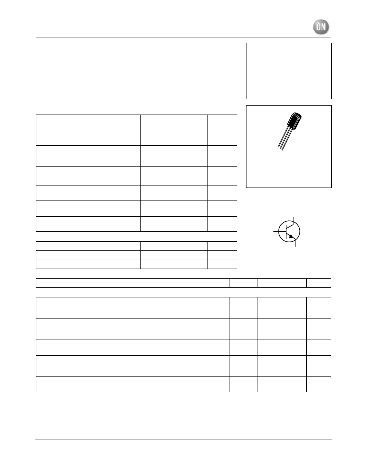
1
2
3
CASE 29–10, STYLE 1
TO–92 (TO–226AE)
COLLECTOR
3
2
BASE
1
EMITTER
Min
Max
Unit
Vdc
30
—
40
—
Vdc
40
—
50
—
5.0
—
Vdc
µAdc
—
0.1
—
0.1
—
0.1
µAdc
Preferred devices are ON Semiconductor recommended choices for future use and best overall value.
© Semiconductor Components Industries, LLC, 2001
1
March, 2001 – Rev. 1
Publication Order Number:
MPSW01/D
Share Link: 