8143RPFB View Datasheet(PDF) - MAXWELL TECHNOLOGIES
Part Name
Description
Manufacturer
8143RPFB Datasheet PDF : 24 Pages
| |||
12-Bit Serial Daisy-Chain D/A Converter
8143
An asynchronous CLEAR function allows resetting the DAC register to a zero code (0000 0000 0000) without altering
data stored in the registers.
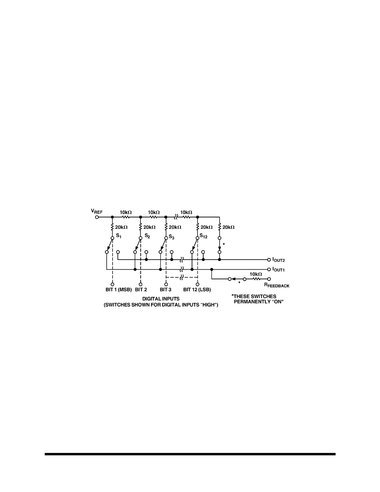
A simplified circuit of the 8143 is shown in Figure 10. An inverses R-2R ladder network consisting of silicon-chrome,
thin-film resistors, and twelve pairs of NMOS current-steering switches. These switches steer binarily weighted cur-
rents into either IOUT1 or IOUT2. Switching current to IOUT1 or IOUT2 yields a constant current in each ladder leg, regard-
less of digital input code. This constant current results in a constant input resistance at VREF equal to R (typically 11
kΩ). The VREF input may be driven by any reference voltage or current, ac or dc, that is within the limits stated in the
Absolute Maximum Ratings chart.
The twelve output current-steering switches are in series with the R-2R resistor ladder, and therefore, can introduce bit
errors. It was essential to design these switches such that the switch “ON” resistance by binarily scaled so that the
voltage drop across each switch remains constant. If, for example, Switch 1 of Figure 10 was designed with an “ON”
resistance of 10 Ω, Switch 2 for 20 Ω, etc., a constant 5 mV drop would then be maintained across each switch.
To further ensure accuracy across the full temperature range, permanently “ON” MOS switches were included in
series with the feedback resistor and the R-2R ladder’s terminating resistor. The Simplified DAC Circuit, Figure 10,
shows the location of these switches. These series switches are equivalently scaled to two times Switch 1 (MSB) and
top Switch 12 (LSB) to maintain constant relative voltage drops with varying temperature. During any testing of the
resistor ladder or RFEEDBACK (such as incoming inspection), VDD must be present to turn “ON” these serial switches.
FIGURE 10. SIMPLIFIED DAC CIRCUIT
ESD Protection
The 8143 digital inputs have been designed with ESD resistance incorporated through careful layout and the inclusion
of input protection circuitry.
Figure 11 shows the input protection diodes. High voltage static charges applied to the digital inputs are shunted to the
supply and ground rails through forward biased diodes.
These protection diodes were designed to clamp the inputs well below dangerous levels during static discharge condi-
tions.
07.23.03 REV 3
All data sheets are subject to change without notice 10
©2003 Maxwell Technologies.
All rights reserved.
Share Link: 