MAX6025 View Datasheet(PDF) - Maxim Integrated
Part Name
Description
Manufacturer
MAX6025 Datasheet PDF : 14 Pages
| |||
Precision, Low-Power, Low-Dropout,
SOT23-3 Voltage References
ABSOLUTE MAXIMUM RATINGS
(Voltages Referenced to GND)
IN .........................................................................-0.3V to +13.5V
OUT .............................................................-0.3V to (VIN + 0.3V)
Output Short Circuit to GND or IN (VIN < 6V) ............Continuous
Output Short Circuit to GND or IN (VIN ≥ 6V) .........................60s
Continuous Power Dissipation (TA = +70°C)
3-Pin SOT23-3 (derate 4.0mW/°C above +70°C) ........320mW
Operating Temperature Range ...........................-40°C to +85°C
Storage Temperature Range .............................-65°C to +150°C
Lead Temperature (soldering, 10s) .................................+300°C
Stresses beyond those listed under “Absolute Maximum Ratings” may cause permanent damage to the device. These are stress ratings only, and functional
operation of the device at these or any other conditions beyond those indicated in the operational sections of the specifications is not implied. Exposure to
absolute maximum rating conditions for extended periods may affect device reliability.
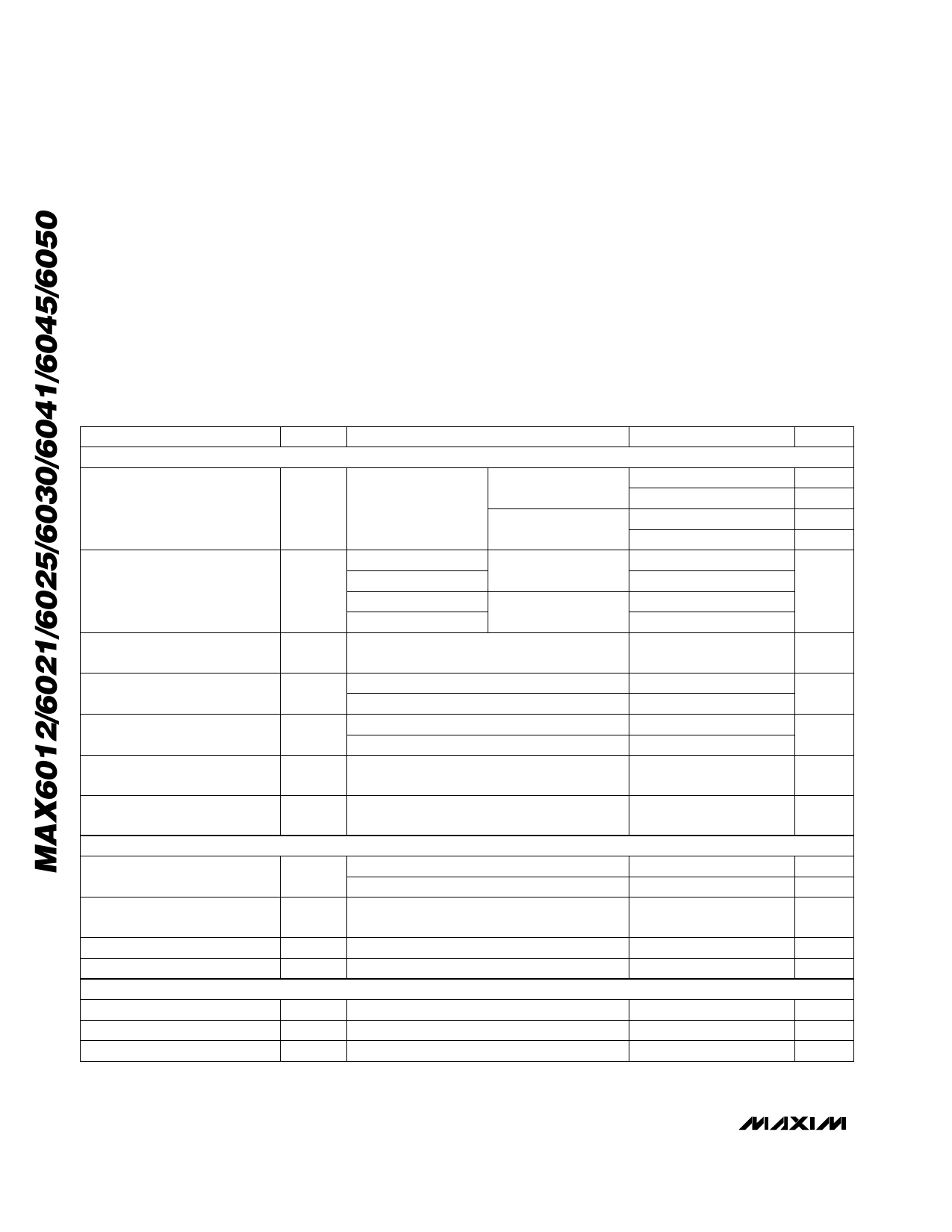
ELECTRICAL CHARACTERISTICS—MAX6012
(VIN = +5V, IOUT = 0, TA = TMIN to TMAX, unless otherwise noted. Typical values are at TA = +25°C.) (Note 1)
PARAMETER
SYMBOL
CONDITIONS
MIN TYP
OUTPUT
Output Voltage
VOUT TA = +25°C
MAX6012A
MAX6012B
1.243
-0.32
1.241
-0.48
1.247
1.247
TA = 0°C to +70°C
MAX6012A
6
Output Voltage Temperature
Coefficient (Note 2)
VOUT
TA = -40°C to +85°C
TA = 0°C to +70°C
MAX6012B
6
6
TA = -40°C to +85°C TA = 0°C to +70°C
6
Line Regulation
∆VOUT/
∆VIN
2.5V ≤ VIN ≤ 12.6V
8
Load Regulation
∆VOUT/ Sourcing: 0 ≤ IOUT ≤ 500µA
∆IOUT Sinking: -500µA ≤ IOUT ≤ 0
0.12
0.15
Short to GND
4
OUT Short-Circuit Current
ISC
Short to IN
4
Temperature Hysteresis
(Note 3)
130
Long-Term Stability
∆VOUT/
time
1000hr at TA = +25°C
50
DYNAMIC
f = 0.1Hz to 10Hz
12
Noise Voltage
eOUT f = 10Hz to 10kHz
65
Ripple Rejection
∆VOUT/
∆VIN
VIN = 5V ±100mV, f = 120Hz
86
Turn-On Settling Time
tR
To VOUT = 0.1% of final value, COUT = 50pF
30
Capacitive-Load Stability Range COUT Note 4
0
INPUT
Supply Voltage Range
VIN Guaranteed by line-regulation test
2.5
Quiescent Supply Current
IIN
27
Change in Supply Current
IIN/VIN 2.5V ≤ VIN ≤ 12.6V
0.8
MAX UNITS
1.251
0.32
1.253
0.48
15
20
25
30
V
%
V
%
ppm/°C
80
µV/V
0.50
µV/µA
0.60
mA
ppm
ppm/
1000hr
µVp-p
µVRMS
dB
µs
2.2
nF
12.6
V
35
µA
2.0 µA/V
2 _______________________________________________________________________________________
Share Link: 