AD625SE View Datasheet(PDF) - Analog Devices
Part Name
Description
Manufacturer
AD625SE Datasheet PDF : 15 Pages
| |||
AD625
These capacitances may also be incorporated as part of the
external input protection circuit (see section on Input Protec-
tion). As a general practice every effort should be made to
match the extraneous capacitance at Pins 15 and 2, and Pins 1
and 16, to preserve high ac CMR.
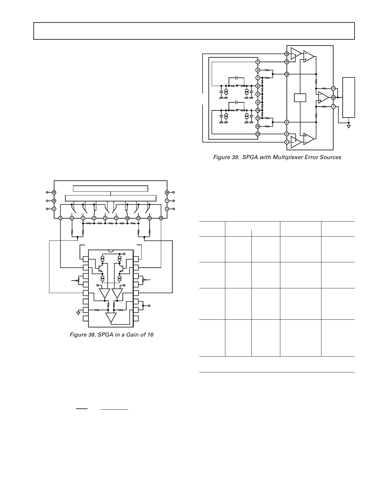
SOFTWARE PROGRAMMABLE GAIN AMPLIFIER
An SPGA provides the ability to externally program precision
gains from digital inputs. Historically, the problem in systems
requiring electronic switching of gains has been the ON resis-
tance (RON) of the multiplexer, which appears in series with the
gain setting resistor RG. This can result in substantial gain errors
and gain drifts. The AD625 eliminates this problem by making
the gain drive and gain sense pins available (Pins 2, 15, 5, 12;
see Figure 39). Consequently the multiplexer’s ON resistance is
removed from the signal current path. This transforms the ON
resistance error into a small nullable offset error. To clarify this
point, an error budget analysis has been performed in Table II
based on the SPGA configuration shown in Figure 39.
AD7502
TTL/DTL TO CMOS LEVEL TRANSLATOR
VSS
A0
VDD
DECODER/DRIVER
A1
GND
EN
20k⍀
3.9k⍀ 975⍀ 650⍀ 975⍀ 3.9k⍀
15.6k⍀
15.6k⍀
+INPUT
–INPUT
20k⍀
1
+GAIN
SENSE
2
RTI NULL
3
+VS
4
RTI NULL
5
+GAIN DRIVE
NC 6
REF
7
–VS 8
A1
A2
10k⍀
10k⍀
10k⍀
10k⍀
A3
AD625
16
–GAIN
SENSE
15
RTO NULL
14
–VS
13
RTO NULL
12
–GAIN DRIVE
11
VOUT
10
9 +VS
Figure 38. SPGA in a Gain of 16
Figure 38 shows an AD625 based SPGA with possible gains of
1, 4, 16, 64. RG equals the resistance between the gain sense
lines (Pins 2 and 15) of the AD625. In Figure 38, RG equals
the sum of the two 975 Ω resistors and the 650 Ω resistor, or
2600 Ω. RF equals the resistance between the gain sense and the
gain drive pins (Pins 12 and 15, or Pins 2 and 5), that is RF
equals the 15.6 kΩ resistor plus the 3.9 kΩ resistor, or 19.5 kΩ.
The gain, therefore equals:
2RF +1= 2(19.5 kΩ) +1=16
RG
(2.6 kΩ)
As the switches of the differential multiplexer proceed synchro-
nously, RG and RF change, resulting in the various programmed
gain settings.
–INPUT
–GAIN
SENSE
CS-OUT
20k⍀ –GAIN
DRIVE
15.6k⍀
RON
3.9k⍀
COUT
IOUT
IS
CS
975k⍀
–
VIN
CS-OUT
650k⍀
+
RON
975k⍀
COUT
IOUT
IS
CS
3.9k⍀
+GAIN
15.6k⍀ DRIVE
20k⍀ +GAIN
SENSE
+INPUT
AD625
10k⍀
10k⍀
VS
10k⍀
10k⍀
12-BIT
DAS
Figure 39. SPGA with Multiplexer Error Sources
Figure 39 shows a complete SPGA feeding a 12-bit DAS with a
0 V–10 V input range. This configuration was used in the error
budget analysis shown in Table II. The gain used for the RTI
calculations is set at 16. As the gain is changed, the ON resis-
tance of the multiplexer and the feedback resistance will change,
which will slightly alter the values in the table.
Table II. Errors Induced by Multiplexer to an SPGA
Induced
Specifications
Error
AD625C AD7520KN Calculation
Voltage Offset
Induced RTI
RTI Offset
Voltage
Gain Sense Switch
Offset
Resistance
Current 170 Ω
40 nA
40 nA × 170 Ω =
6.8 µV
6.8 µV
RTI Offset
Voltage
Gain Sense Differential
Current Switch
60 nA
Resistance
6.8 Ω
60 nA × 6.8 Ω =
0.41 µV
0.41 µV
RTO Offset Feedback
Voltage Resistance
20 kΩ1
Differential 2 (0.2 nA × 20 kΩ)
Leakage = 8 µV/16
Current (IS)2
+0.2 nA
–0.2 nA
0.5 µV
RTO Offset Feedback
Voltage Resistance
20 kΩ1
Differential
Leakage
Current
(IOUT)2
+1 nA
–1 nA
2 (1 nA × 20 kΩ)
= 40 µV/16
2.5 µV
Total error induced by a typical CMOS multiplexer
to an SPGA at +25°C
10.21 A
NOTES
1The resistor for this calculation is the user-provided feedback resistance (RF).
20 kΩ is recommended value (see Resistor Programmable Gain Amplifier section).
2The leakage currents (IS and IOUT) will induce an offset voltage, however, the offset
will be determined by the difference between the leakages of each “half’’ of the
differential multiplexer. The differential leakage current is multiplied by the
feedback resistance (see Note 1), to determine offset voltage. Because differential
leakage current is not a parameter specified on multiplexer data sheets, the most
extreme difference (one most positive and one most negative) was used for the
calculations in Table II. Typical performance will be much better.
**The frequency response and settling will be affected by the ON resistance and
internal capacitance of the multiplexer. Figure 40 shows the settling time vs.
ON resistance at different gain settings for an AD625 based SPGA.
**Switch resistance and leakage current errors can be reduced by using relays.
REV. D
–13–
Share Link: 