81C56 View Datasheet(PDF) - Intersil
Part Name
Description
Manufacturer
81C56 Datasheet PDF : 11 Pages
| |||
HS-81C55RH, HS-81C56RH
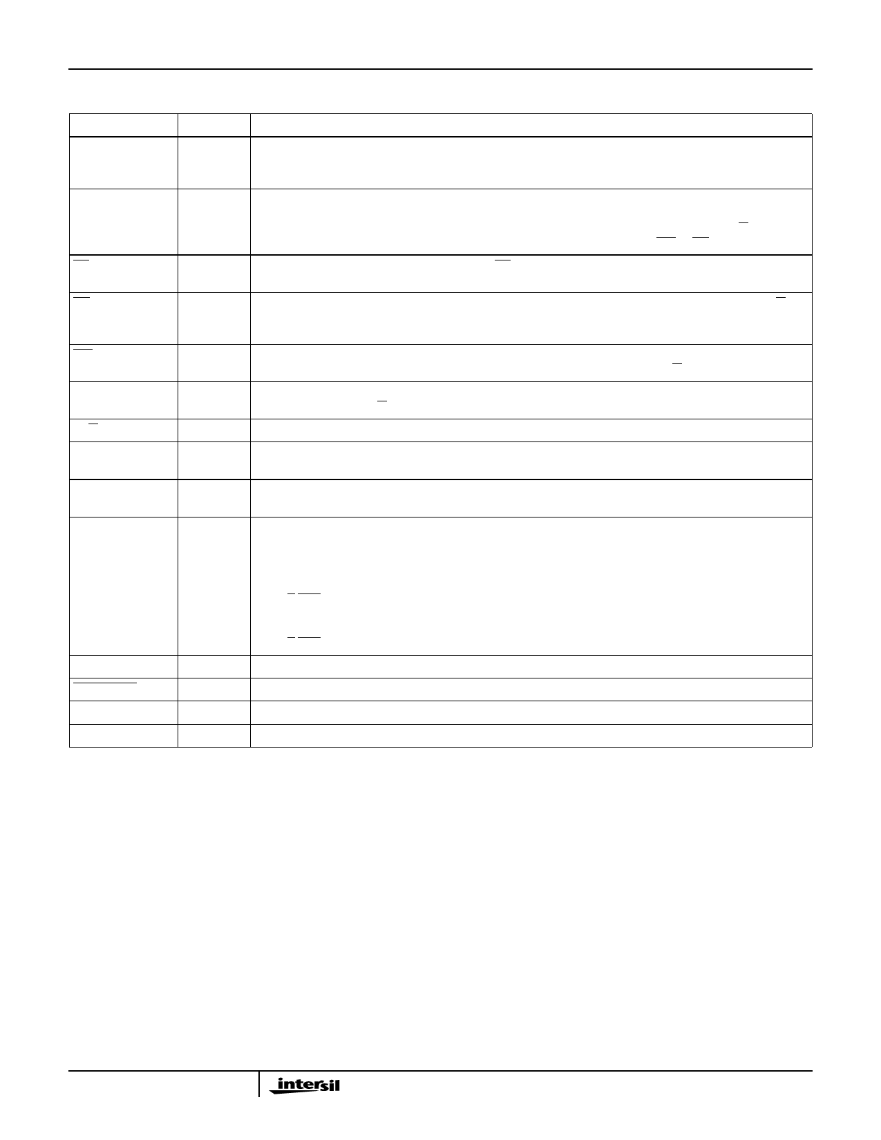
Pin Descriptions
SYMBOL
TYPE
RESET
I
AD0 - AD7
I/O
CE or CE
I
RD
I
WR
I
ALE
I
IO/M
I
PA0 - PA7 (8)
I/O
PB0 - PB7 (8)
I/O
PC0 - PC7 (8)
I/O
TIMER IN
I
TIMER OUT
O
VDD
I
GND
I
NAME AND FUNCTION
Reset: Pulse provided by the HS-80C85RH to initialize the system (connect to HS-80C85RH RESET OUT).
Input high on this line resets the chip and initializes the three I/O ports to input mode. The width of RESET
pulse should typically be two HS-80C85RH clock cycle times.
Address/Data: Three-state Address/Data lines that interface with the CPU lower 8-bit Address/Data Bus. The
8-bit address is latched into the address latch inside the HS-81C55 and HS-81C56RH on the falling edge of
ALE. The address can be either for the memory section or the I/O section depending on the IO/M input. The
8-bit data is either written into the chip or read from the chip, depending on the WR or RD input signal.
Chip Enable: On the HS-81C55RH, this pin is CE and is ACTIVE LOW. On the HS-81C56RH, this pin is CE
and is ACTIVE HIGH.
Read Control: Input low on this line with the Chip Enable active enables and AD0 - AD7 buffers. If IO/M pin
is low, the RAM content will be read out to the AD bus. Otherwise the content of the selected I/O port or
command/status registers will be read to the AD bus.
Write Control: Input low on this line with the Chip Enable active causes the data on the Address/Data bus to
be written to the RAM or I/O ports and command/status register, depending on IO/M.
Address Latch Enable: This control signal latches both the address on the AD0 - AD7 lines and the state of
the Chip Enable and IO/M into the chip at the falling edge of ALE.
I/O Memory: Selects memory if low and I/O and command/status registers if high.
Port A: These 8 pins are general purpose I/O pins. The in/out direction is selected by programming the
command register.
Port B: These 8 pins are general purpose I/O pins. The in/out direction is selected by programming the
command register.
Port C: These 6 pins can function as either input port, output port, or as control signals for PA and PB.
Programming is done through the command register. When PC0 - PC5 are used as control signals, they will
provide the following:
PC0 - A INTR (Port A Interrupt)
PC1 - ABF (Port A Buffer Full)
PC2 - A STB (Port A Strobe)
PC3 - B INTR (Port B Interrupt)
PC4 - B BF (Port B Buffer Full)
PC5 - B STB (Port B Strobe)
Timer Input: Input to the counter-timer.
Timer Output: This output can be either a square wave or a pulse, depending on the timer mode.
Voltage: +5V.
Ground: Ground reference.
3
Share Link: 