81C56 View Datasheet(PDF) - Intersil
Part Name
Description
Manufacturer
81C56 Datasheet PDF : 11 Pages
| |||
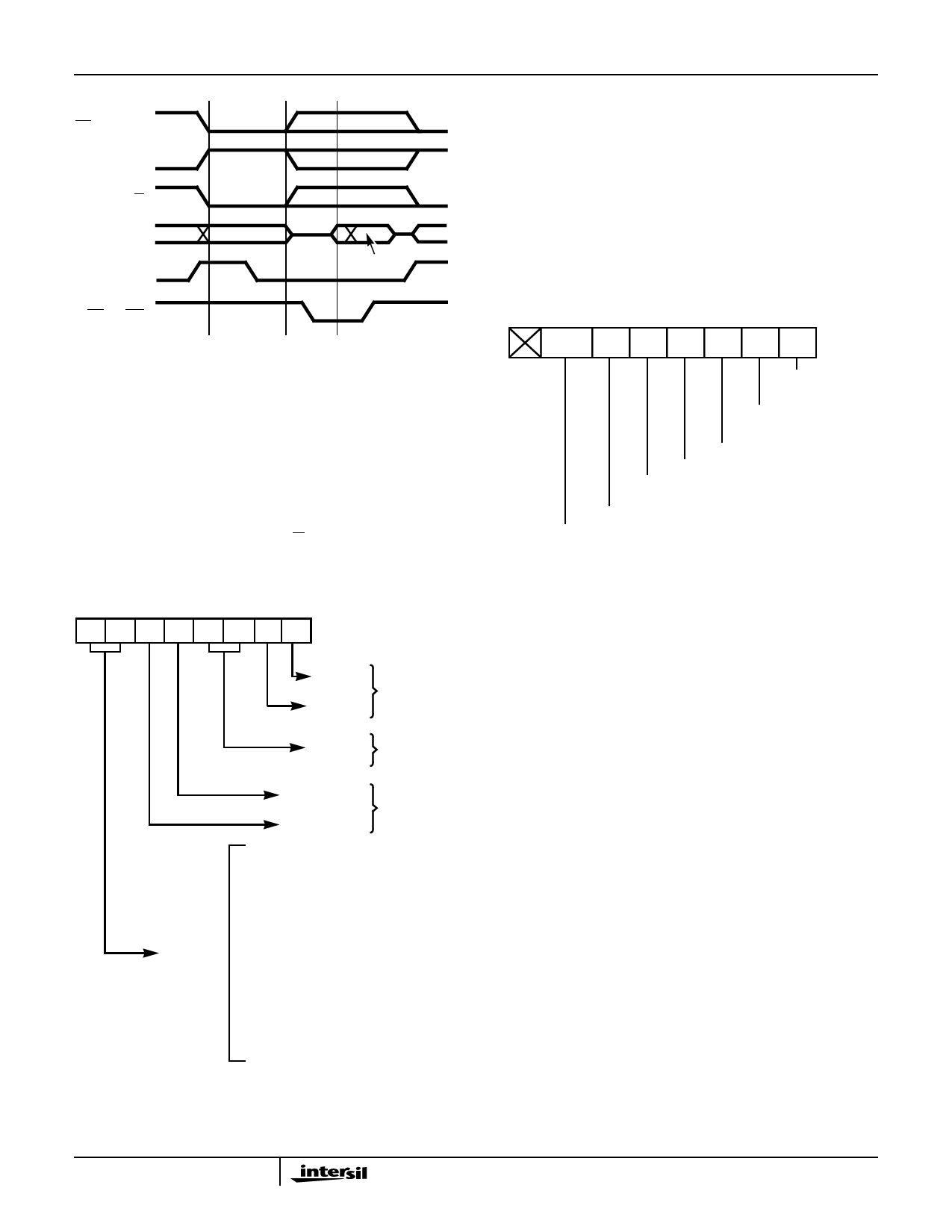
HS-81C55RH, HS-81C56RH
CE (81C55RH)
OR
CE (81C56RH)
IO/M
AD0 - AD7
ALE
ADDRESS
DATA
VALID
RD OR WR
FIGURE 2. ON-BOARD MEMORY READ/WRITE CYCLE
Programming of the Command Register
The command register consists of eight latches. Four bits (0-
3) define the mode of the ports, two bit (4-5) enable or disable
the interrupt from port C when it acts as control port, and the
last two bits (6-7) are for the timer.
The command register contents can be altered at anytime by
using the I/O address XXXXX000 during a WRITE operation
with the Chip Enable active and IO/M = 1. The meaning of
each bit of the command byte is defined in Figure 3. The
contents of the command register may never be read.
76543210
TM2 TM1 IEB IEA PC2 PC1 PB PA
TIMER
COMMAND
DEFINES
PA0 - PA7
DEFINES
PB0 - PB7
DEFINES
PC0 - PC5
0 = INPUT
1 = OUTPUT
00 = ALT1
11 = ALT2
01 = ALT3
10 = ALT4
ENABLE PORT
A INTERRUPT
ENABLE PORT
B INTERRUPT
0 = INPUT
1 = OUTPUT
00 = NOP - DO NOT AFFECT COUNTER
OPERATION
01 = STOP - NOP IF TIMER HAS NOT
STARTED; STOP COUNTING IF
THE TIMER IS RUNNING
10 = STOP AFTER TC - STOP IMME-
DIATELY AFTER PRESENT TC
IS REACHED (NOP IF TIMER
HAS NOT STARTED)
11 = START - LOAD MODE AND CNT
LENGTH AND START IMMEDIATE-
LY AFTER LOADING (IF TIMER IS
NOT PRESENTLY RUNNING). IF
TIMER IS RUNNING, START THE
NEW MODE AND CNT LENGTH
IMMEDIATELY AFTER PRESENT
TC IS REACHED.
FIGURE 3. COMMAND REGISTER BIT ASSIGNMENT
Reading the Status Register
The status register consists of seven latches, one for each
bit six (0-5) for the status of the ports and one (6) for the
status of the timer.
The status of the timer and the I/O section can be polled by
reading the Status Register (Address XXXXX000). Status
word format is shown in Figure 4. Note that you may never
write to the status register since the command register
shares the same I/O address and the command register is
selected when a write to that address is issued.
AD7 AD6 AD5 AD4 AD3 AD2 AD1 AD0
TIMER
INTE
B
B
BF
INTR INTE
BA
A
BF
INTR
A
PORT A
INTERRUPT
REQUEST
PORT A BUFFER
FULL/EMPTY
(INPUT/OUTPUT)
PORT A INTERRUPT ENABLE
PORT B INTERRUPT REQUEST
PORT B BUFFER FULL/EMPTY
(INPUT/OUTPUT)
PORT B INTERRUPT ENABLE
TIMER INTERRUPT (THIS BIT IS LATCHED HIGH WHEN
TERMINAL COUNT IS REACHED, AND IS RESET TO LOW
READING OF THE C/S REGISTER & BY HARDWARE RESET).
FIGURE 4. STATUS REGISTER BIT ASSIGNMENT
Input/Output Section
The I/O section of the HS-81C55RH and HS-81C56RH
consists of five registers: (See Figure 5)
• Command/Status Register (C/S) - Both register are
assigned the address XXXXX000. The C/S address
serves the dual purpose.
When the C/S registers are selected during WRITE
operation, a command is written into the command
register. The contents of this register are not accessible
through the pins.
When the C/S (XXXXX000) is selected during a READ
operation, the status information of the I/O ports and
the timer becomes available on the AD0 - AD7 lines.
• PA Register - This register can be programmed to be
either input or output ports depending on the status of
the contents of the C/S Register. also depending on the
command, this port can operate in either the basic
mode or the strobed mode (See timing diagram). the
I/O pins assigned in relation to this register are PA0 -
PA7. The address of this register is XXXXX001.
• PB Register - This register functions the same as PA
Register. the I/O pins assigned are PB0 - PB7. The
address of this register is XXXXX010
• PC Register - This register has the address
XXXXX011 and contains only 6 bits. The 6 bits can be
programmed to be either input ports, output ports or as
7
Share Link: 