81C56 View Datasheet(PDF) - Intersil
Part Name
Description
Manufacturer
81C56 Datasheet PDF : 11 Pages
| |||
HS-81C55RH, HS-81C56RH
control signals for PA and PB by properly programming
the AD2 and AD3 bits of the C/S register.
When PC0 - PC5 is used as a control port, 3 bits are
assigned for Port A and 3 for Port B. The first bit is an
Interrupt that the HS-81C55RH and HS-81C56RH sends
out. The second is an output signal indicating whether the
buffer is full or empty, and the third is an input pin to
accept a strobe for the strobed input mode. (See Table 1).
When the ‘C’ port is programmed to either ALT3 or ALT4, the
control signals for PA and PB are initialized as follows:
CONTROL
BF
INTR
STB
INPUT MODE
Low
Low
Input Control
OUTPUT MODE
Low
High
Input Control
When in the ALT1 or ALT2 modes, the bits of Port C are
structured like the diagram above in the simple input or
output mode, respectively.
Reading from an input port with nothing connected to the
pins will provide unpredictable results.
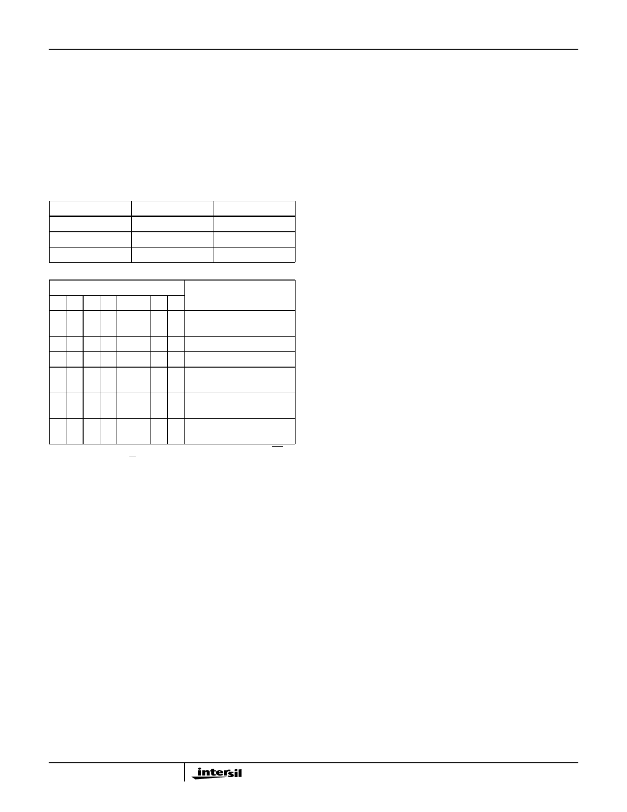
I/O ADDRESS†
A7 A6 A5 A4 A3 A2 A1 A0
SELECTION
X X X X X 0 0 0 Interval Command/
Status Register
X X X X X 0 0 1 General Purpose I/O Port A
X X X X X 0 1 0 General Purpose I/O Port B
X X X X X 0 1 1 General Purpose I/O or
Control Port C
X X X X X 1 0 0 Low-Order 8 Bits of
Timer Count
X X X X X 1 0 1 High 6 Bits of Timer Count
and 2 Bits of Timer Mode
† I/O Address must be qualified by CE = 1(81C56RH) or CE =
0(81C55RH) and IO/M = 1 in order to select the appropriate register.
X = Don’t Care
FIGURE 5. I/O PORT AND TIMER ADDRESSING SCHEME
Figure 6 shows how I/O Ports A and B are structured within
the HS-81C55RH and HS-81C56RH.
Note in the diagram that when the I/O ports are programmed
to be output ports, the contents of the output ports can still
be read by a READ operation when appropriately
addressed.
The outputs of the HS-81C55/56RH are “glitch-free”
meaning that you can write a “1” to a bit position that was
previously “1” and the level at the output pin will not change.
Note also that the output latch is cleared when the port
enters the input mode. the output latch cannot be loaded by
writing to the port if the port is in the input mode. The result
is that each time a port mode is changed from input to
output, the output pins will go low. When the HS-
81C55/56RH is RESET, the output latches are all cleared
and all 3 ports enter the input mode.
8
Share Link: 