ADM1024(2000) View Datasheet(PDF) - Analog Devices
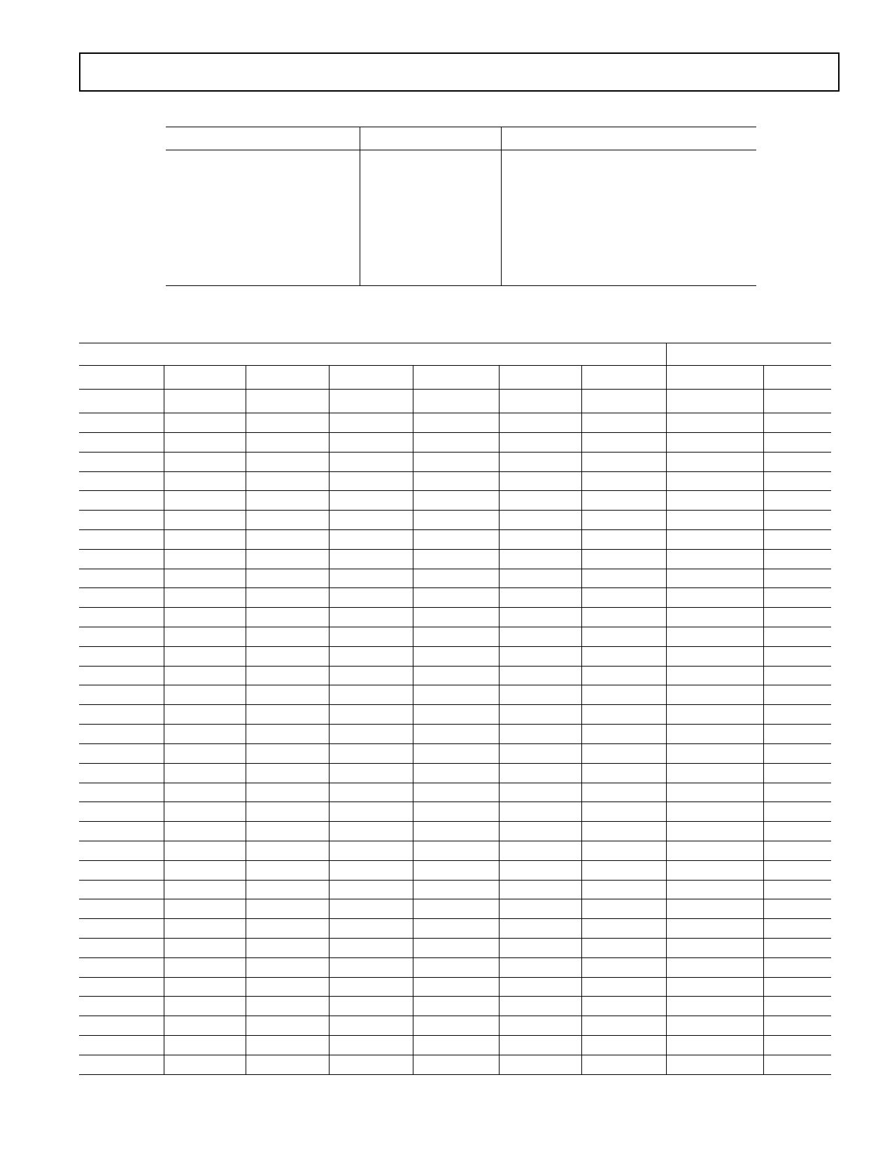
Part Name
Description
Manufacturer
ADM1024 Datasheet PDF : 28 Pages
| |||
ADM1024
A-TO-D CONVERTER
These inputs are multiplexed into the on-chip, successive
approximation, analog-to-digital converter. This has a resolution
of eight bits. The basic input range is zero to 2.5 V, which is
the input range of AIN1 and AIN2, but five of the inputs have
built-in attenuators to allow measurement of 2.5 V, 5 V, 12 V
and the processor core voltages VCCP1 and VCCP2, without any
external components. To allow for the tolerance of these supply
voltages, the A-to-D converter produces an output of 3/4 full-scale
(decimal 192) for the nominal input voltage, and so has adequate
headroom to cope with overvoltages. Table III shows the input
ranges of the analog inputs and output codes of the A-to-D
converter.
When the ADC is running, it samples and converts an input
every 748 µs, except for the external temperature (D1 and D2)
inputs. These have special input signal conditioning and are
averaged over 16 conversions to reduce noise, and a measure-
ment on one of these inputs takes nominally 9.6 ms.
INPUT CIRCUITS
The internal structure for the analog inputs are shown in Figure
10. Each input circuit consists of an input protection diode,
an attenuator, plus a capacitor to form a first-order low-pass
filter which gives the input immunity to high frequency noise.
AIN1–AIN2
80k⍀
+12V
+5V
+2.5VIN
(SEE TEXT)
+VCCP1/
VCCP2
122.2k⍀
22.7k⍀
91.6k⍀
55.2k⍀
36.7k⍀
111.2k⍀
42.7k⍀
97.3k⍀
10pF
35pF
25pF MUX
25pF
50pF
R1 = (VFS – 2.5)
R2
2.5
Negative and bipolar input ranges can be accommodated by
using a positive reference voltage to offset the input voltage range
so it is always positive.
To measure a negative input voltage, an attenuator can be used
as shown in Figure 12.
+VOS
R2
R1
VIN
AIN (1–2)
Figure 12. Scaling and Offsetting AIN(1–2) for Negative
Inputs
R1 = |VFS– |
R2 VOS
This is a simple and cheap solution, but the following point
should be noted. Since the input signal is offset but not inverted,
the input range is transposed. An increase in the magnitude of
the –12 V supply (going more negative), will cause the input
voltage to fall and give a lower output code from the ADC.
Conversely, a decrease in the magnitude of the –12 V supply will
cause the ADC code to increase. The maximum negative voltage
corresponds to zero output from the ADC. This means that the
upper and lower limits will be transposed.
Bipolar input ranges can easily be accommodated. By making R1
equal to R2 and VOS = 2.5 V, the input range is ±2.5 V. Other input
ranges can be accommodated by adding a third resistor to set the
positive full-scale input voltage.
+VOS
R2
R1
AIN (1–2)
VIN
R3
Figure 10. Structure of Analog Inputs
Figure 13. Scaling and Offsetting AIN(1–2) for Bipolar Inputs
2.5 V INPUT PRECAUTIONS
When using the 2.5 V input, the following precautions should
be noted. There is a parasitic diode between Pin 18 and VCC
due to the presence of a PMOS current source (which is used
when Pin 18 is configured as a temperature input). This will
become forward-biased if Pin 18 is more than 0.3 V above VCC.
Therefore, VCC should never be powered off with a 2.5 V input
connected.
SETTING OTHER INPUT RANGES
AIN1 and AIN2 can easily be scaled to voltages other than 2.5 V.
If the input voltage range is zero to some positive voltage, all
that is required is an input attenuator, as shown in Figure 11.
R1 = |VFS– |
R2 R2
(R3 has no effect as the input voltage at the device Pin is zero
when VIN = minus full-scale.)
R1 = (VFS+ – 2.5)
R3
2.5
(R2 has no effect as the input voltage at the device pin is 2.5 V
when VIN = plus full-scale).
Offset voltages other than 2.5 V can be used, but the calculation
becomes more complicated.
R1 AIN (1–2)
VIN
R2
Figure 11. Scaling AIN(1–2)
TEMPERATURE MEASUREMENT SYSTEM
Internal Temperature Measurement
The ADM1024 contains an on-chip bandgap temperature sensor,
whose output is digitized by the on-chip ADC. The temperature
data is stored in the Temperature Value Register (address 27h)
and the LSB from Bits 6 and 7 of the Temperature Configuration
REV. 0
–11–
Share Link: 