ADM1021AARQ View Datasheet(PDF) - Analog Devices
Part Name
Description
Manufacturer
ADM1021AARQ Datasheet PDF : 16 Pages
| |||
ADM1021A
2. Data is sent over the serial bus in sequences of nine clock
pulses, eight bits of data followed by an Acknowledge Bit
from the slave device. Transitions on the data line must occur
during the low period of the clock signal and remain stable
during the high period, as a low-to-high transition when the
clock is high may be interpreted as a stop signal. The number
of data bytes that can be transmitted over the serial bus in a
single read or write operation is limited only by what the
master and slave devices can handle.
3. When all data bytes have been read or written, stop conditions
are established. In write mode, the master will pull the data line
high during the 10th clock pulse to assert a stop condition. In
read mode, the master device will override the acknowledge bit
by pulling the data line high during the low period before the
ninth clock pulse. This is known as No Acknowledge. The
master will then take the data line low during the low period
before the 10th clock pulse, then high during the 10th clock
pulse to assert a stop condition.
Any number of bytes of data may be transferred over the serial
bus in one operation, but it is not possible to mix read and write
in one operation, because the type of operation is determined at
the beginning and cannot subsequently be changed without
starting a new operation.
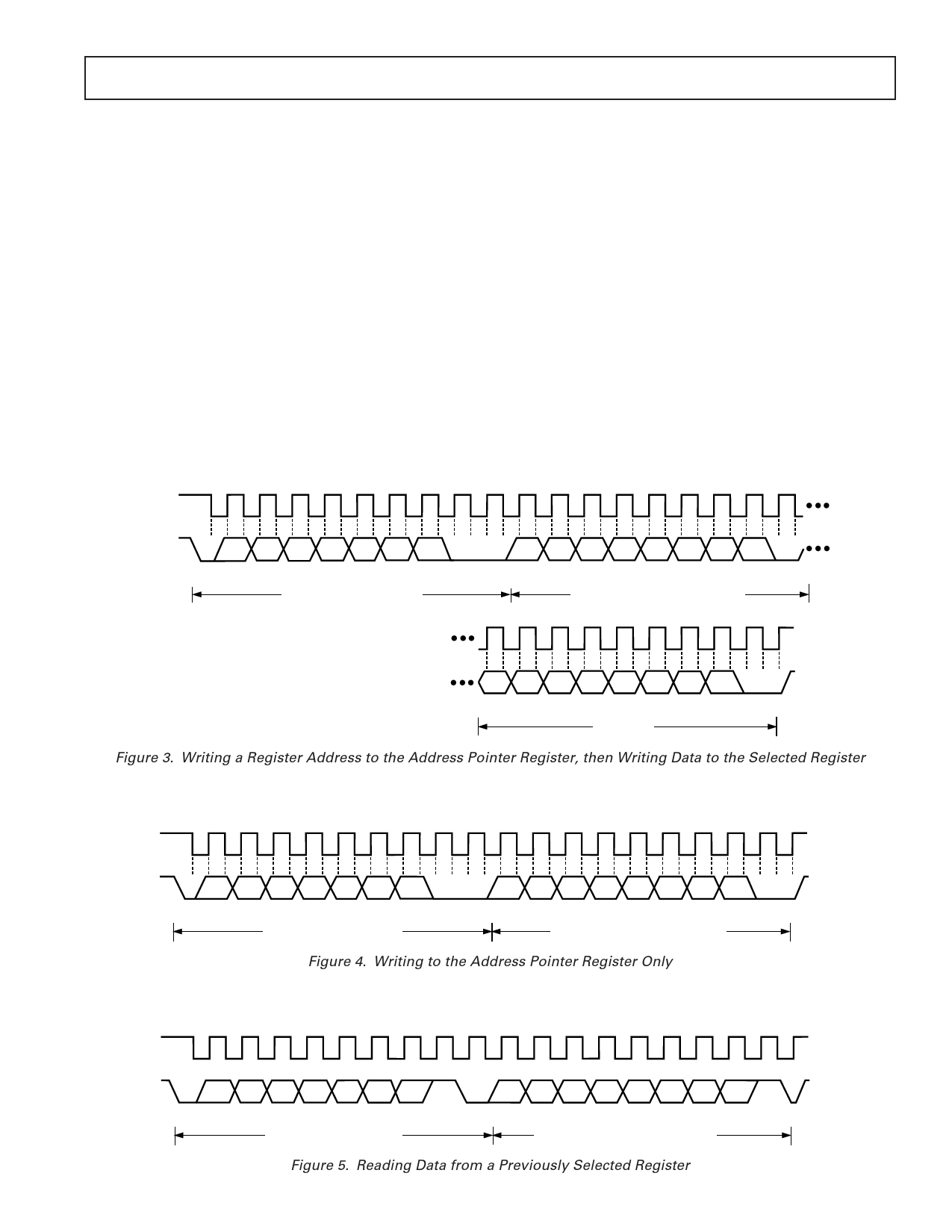
In the case of the ADM1021A, write operations contain either
one or two bytes, while read operations contain one byte.
To write data to one of the device data registers or read data
from it, the Address Pointer Register must be set so that the
correct data register is addressed, data can then be written into
that register or read from it. The first byte of a write operation
always contains a valid address that is stored in the Address
Pointer Register. If data is to be written to the device, the write
operation contains a second data byte that is written to the reg-
ister selected by the address pointer register.
1
9
1
9
SCLK
SDATA
A6
START BY
MASTER
A5 A4 A3 A2 A1 A0 R/W
D7
FRAME 1
SERIAL BUS ADDRESS BYTE
ACK. BY
ADM1021A
1
SCL (CONTINUED)
D6 D5 D4 D3 D2 D1 D0
FRAME 2
ADDRESS POINTER REGISTER BYTE
ACK. BY
ADM1021A
9
SDA (CONTINUED)
D7 D6 D5 D4 D3 D2 D1 D0
FRAME 3
DATA BYTE
ACK. BY
ADM1021A
STOP BY
MASTER
Figure 3. Writing a Register Address to the Address Pointer Register, then Writing Data to the Selected Register
1
9
1
9
SCLK
SDATA
A6
START BY
MASTER
A5 A4 A3 A2 A1 A0
FRAME 1
SERIAL BUS ADDRESS BYTE
R/W
D7
ACK. BY
ADM1021A
D6 D5 D4 D3 D2 D1 D0
FRAME 2
ADDRESS POINTER REGISTER BYTE
ACK. BY
ADM1021A
Figure 4. Writing to the Address Pointer Register Only
STOP BY
MASTER
1
9
1
9
SCLK
SDATA
A6
START BY
MASTER
REV. D
A5 A4 A3 A2 A1 A0
FRAME 1
SERIAL BUS ADDRESS BYTE
R/W
D7
ACK. BY
ADM1021A
D6 D5 D4 D3 D2 D1 D0
NO ACK.
BY MASTER
FRAME 2 DATA BYTE FROM ADM1021A
Figure 5. Reading Data from a Previously Selected Register
–9–
STOP BY
MASTER
Share Link: 