G768B View Datasheet(PDF) - Global Mixed-mode Technology Inc
Part Name
Description
Manufacturer
G768B
Global Mixed-mode Technology Inc

G768B Datasheet PDF : 15 Pages
| |||
Global Mixed-mode Technology Inc.
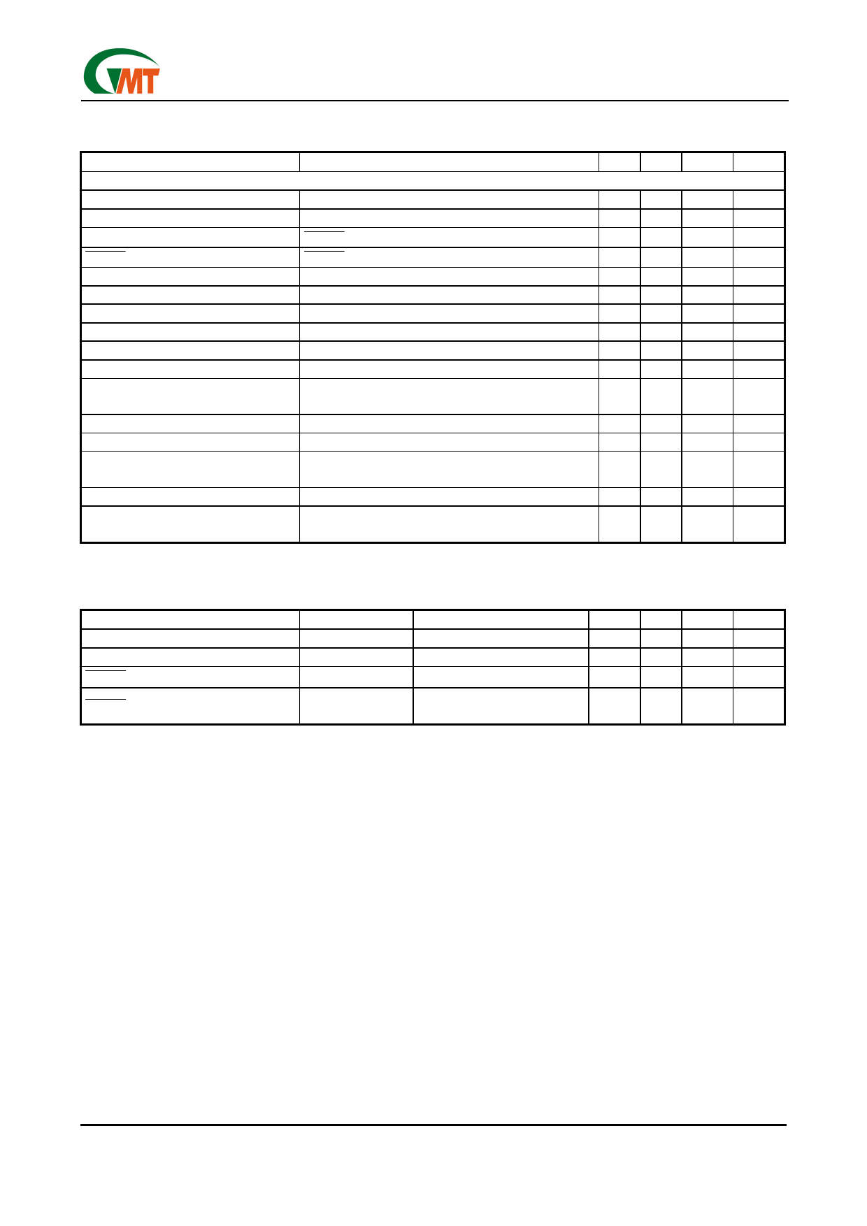
Electrical Characteristics (continued)
(Vcc = + 5V, TA = 60°C, unless otherwise noted.)
PARAMETER
SMBus Interface
Logic Input High Voltage
Logic Input Low Voltage
Logic Output Low Sink Current
ALERT Output High Leakage Current
Logic Input Current
SMBus Input Capacitance
SMBus Clock Frequency
SMBCLK Clock Low Time
SMBCLK Clock High Time
SMBus Start-Condition Setup Time
SMBus Repeated Start-Condition
Setup Time
SMBus Start-Condition Hold Time
SMBus Start-Condition Setup Time
SMBus Data Valid to SMBCLK Ris-
ing-Edge Time
SMBus Data-Hold Time
SMBCLK Falling Edge to SMBus
Data-Valid Time
CONDITIONS
SMBCLK, SMBDATA; Vcc = 4.5V to 5.5V
SMBCLK, SMBDATA; Vcc = 4.5V to 5.5V
ALERT , SMBDATA forced to 0.4V
ALERT forced to 5.5V
Logic inputs forced to Vcc or GND
SMBCLK, SMBDATA
(Note 4)
tLOW , 10% to 10% points
tHIGH , 90% to 90% points
tSU : STA , 90% to 90% points
tHD: STA , 10% of SMBDATA to 90% of SMBCLK
tSD: STO , 90% of SMBDATA to 10% of SMBDATA
tSU: DAT , 10% or 90% of SMBDATA to 10% of
SMBCLK
tHD : DAT(Note 5)
Master clocking in data
G768B
MIN TYP MAX UNITS
2.4
6
-2
5
DC
4.7
4
4.7
500
V
0.8
V
mA
1
µA
2
µA
pF
100 kHz
µs
µs
µs
ns
4
µs
4
µs
800
ns
0
µs
1
µs
Electrical Characteristics (continued)
(VCC =full range, TA= 60°C, unless otherwise noted.)
PARAMETER
Reset Threshold
Reset Active Timeout Period
RESET Output Voltage Low
RESET Output Voltage High
SYMBOL
VTH
VOL
VOH
CONDITIONS
VCC=VTH min ISINK =3.2mA
VCC>VTH max
ISOURCE =5.0mA
MIN TYP MAX UNITS
4.2 4.4 4.5
V
340
ms
0.4
V
VCC-1.5
V
Note 1: Guaranteed but not 100% tested.
Note 2: Quantization error is not included in specifications for temperature accuracy. For example, if the G768B
device temperature is exactly +66.7°C, or +68°C (due to the quantization error plus the +1/2°C offset
used for rounding up) and still be within the guaranteed ±3°C error limits for the +60°C to +100°C tem-
perature range. See Table3.
Note 3: A remote diode is any diode-connected transistor from Table1. TR is the junction temperature of the re-
mote diode. See Remote Diode Selection for remote diode forward voltage requirements.
Note 4: The SMBus logic block is a static design that works with clock frequencies down to DC. While slow op-
eration is possible, it violates the 10kHz minimum clock frequency and SMBus specifications, and may
monopolize the bus.
Note 5: Note that a transition must internally provide at least a hold time in order to bridge the undefined region
(300ns max) of SMBCLK's falling edge.
Ver 1.3
Oct 28, 2002
TEL: 886-3-5788833
http://www.gmt.com.tw
4
Share Link: