AD724JR View Datasheet(PDF) - Analog Devices
Part Name
Description
Manufacturer
AD724JR Datasheet PDF : 15 Pages
| |||
AD724
Both the analog and digital ground pins should be tied to the
ground plane by a short, low inductance path. Each power
transmitted. Each output requires a 220 µF series capacitor to
work with the 75 Ω resistance to pass these low frequencies. The
supply pin should be bypassed to ground by a low inductance
CRMA signal has information mostly up at the chroma fre-
0.1 µF capacitor and a larger tantalum capacitor of about 10 µF. quency and can use a smaller capacitor if desired, but 220 µF
The three analog inputs (RIN, GIN, BIN) should be terminated
with 75 Ω to ground close to the respective pins. However, as
can be used to minimize the number of different components
used in the design.
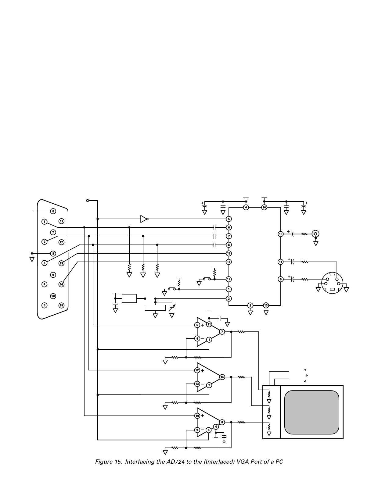
these are high impedance inputs, they can be in a loop-through Displaying VGA Output on a TV
configuration. This technique is used to drive two or more
The AD724 can be used to convert the analog RGB output from a
devices with high frequency signals that are separated by some
personal computer’s VGA card to the NTSC or PAL television
distance. A connection is made to the AD724 with no local
standards. To accomplish this it is important to understand that
termination, and the signals are run to another distant device
the AD724 requires interlaced RGB video and clock rates that
where the termination for these signals is provided.
are consistent with those required by the television standards. In
The output amplitudes of the AD724 are double that required
by the devices that it drives. This compensates for the halving of
most computers the default output is a noninterlaced RGB
signal at a frame rate higher than used by either NTSC or PAL.
the signal levels by the required terminations. A 75 Ω series
resistor is required close to each AD724 output, while 75 Ω to
Most VGA controllers support a wide variety of output modes
that are controlled by altering the contents of internal registers.
ground should terminate the far end of each line.
It is best to consult with the VGA controller manufacturer to
The outputs have a dc bias and must be ac coupled for proper
operation. The COMP and LUMA outputs have information
determine the exact configuration required to provide an inter-
laced output at 60 Hz (50 Hz for PAL).
down to 30 Hz for NTSC (25 MHz for PAL) that must be
SELECT
+5V
+5V
10F 0.1F
0.1F 10F
APOS DPOS
+5V
0.1F
75⍀ 75⍀
75⍀
+5V
JMP 10k⍀
OSC * *
* CRYSTAL
10–30pF
***
0.1F
0.1F
0.1F
+5V
JMP 10k⍀
ENCD
RIN
GIN
CMPS
BIN AD724
HSYNC
VSYNC
LUMA
SELECT
CRMA
+5V (VAA)
0.1F
STND
FIN AGND DGND
75⍀
220F
75⍀
220F
75⍀
220F
COMPOSITE
VIDEO
Y
C
S-VIDEO
(Y/C VIDEO)
VGA OUTPUT
CONNECTOR
1/3
AD8013
649⍀
649⍀
75⍀
* PARALLEL–RESONANT
CRYSTAL; 3.579545MHz (NTSC)
OR 4.433620MHz (PAL)
CAPACITOR VALUE DEPENDS ON
CRYSTAL CHOSEN
**FSC OR 4FSC CLOCK; 3.579545MHz,
14.31818MHz (NTSC) OR 4.433620MHz,
17.734480MHz(PAL)
*** 0.1F CAPACITORS RECOMMENDED
1/3
75⍀
AD8013
VSYNC
FROM VGA PORT
HSYNC
649⍀
649⍀
B
75⍀
G
75⍀
1/3
75⍀
AD8013
R
75⍀
649⍀
–5V
649⍀
RGB MONITOR
Figure 15. Interfacing the AD724 to the (Interlaced) VGA Port of a PC
–10–
REV. B
Share Link: 